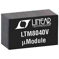
LTM8040IV#PBF Linear Technology, LTM8040IV#PBF Datasheet - Page 6

LTM8040IV#PBF
Manufacturer Part Number
LTM8040IV#PBF
Description
IC, LED DRIVER/CURRENT SOURCE, LGA-66
Manufacturer
Linear Technology
Datasheet
1.LTM8040IVPBF.pdf
(20 pages)
Specifications of LTM8040IV#PBF
Led Driver Application
Automotive, Avionic Lighting
No. Of Outputs
1
Output Current
1A
Output Voltage
13V
Input Voltage
4V To 36V
Dimming Control Type
PWM
Topology
Buck
Lead Free Status / RoHS Status
Lead free / RoHS Compliant
Lead Free Status / RoHS Status
Lead free / RoHS Compliant
Available stocks
Company
Part Number
Manufacturer
Quantity
Price
LTM8040
LEDA (Bank 1): This pin is the regulated current source
of the LTM8040. Connect the anode of the LED string to
this pin. This voltage must be at least 2.5V for accurate
current regulation.
SHDN (Pin L4): The SHDN pin is used to shut down the
switching regulator and the internal bias circuits. The
2.65V switching threshold can function as an accurate
undervoltage lockout. Pull below 0.3V to shut down the
LTM8040. Pull above 2.65V to enable the LTM8040. Tie
to V
BIAS (Pin L5): The BIAS pin connects through an internal
Schottky diode to provide power to internal housekeeping
circuits. Connect to a voltage source (usually LPWR or V
greater than 2.6V. Note that this pin is adjacent to the LPWR
pin to ease layout. If this pin is powered by an external
power source, a decoupling cap may be necessary.
LPWR (Pin K5): This is the output of the buck regulator
that sources the LED current. If the LEDA voltage is above
2.6V, connect this pin to BIAS. It is pinned out primarily
for the convenience of the user. If it is not used, leave this
pin fl oating. Please refer to the Applications Information
section for details.
PWM (Pin L7): Input Pin for PWM Dimming Control. A
PWM signal above 1.2V (ON threshold) turns on the output
current source, while a PWM signal below 0.4V shuts it
down. If the application does not require PWM dimming,
then the PWM pin can be left either open (an internal 10μA
source current pulls PWM high) or pulled up to a voltage
source between 1.2V and 10V.
PIN FUNCTIONS
6
IN
if the SHDN function is unused.
IN
)
V
internal power converter and other circuitry. It must be lo-
cally bypassed with a high quality (low ESR) capacitor.
ADJ (Pin L3): Use the ADJ pin to scale the LEDA output
current below 1A by either applying a voltage source or by
connecting a resistor to GND. This pin is internally pulled
up to a 1.25V reference through a 5.11k resistor, so ensure
that the voltage source can drive a 5.11k impedance. If
applying a voltage to ADJ, the LEDA current follows the
formula: I
GND, the resistor value should be R = 5.11 • I
– I
out of LEDA in amps. Make sure that the voltage at LEDA
is at least 2.5V.
RT (Pin L2): The RT pin is used to set the internal oscillator
frequency. An 80.6k resistor has already been installed
inside the LTM8040 to default switching frequency to
500kHz. If no modifi cation of the switching frequency is
necessary, leave this pin fl oating. Otherwise, a parallel
resistor applied from RT to GND will raise the switching
frequency. See Table 1 for details.
GND (Bank 2, Pin L1): Tie all GND pins directly to a local
ground plane. These pins serve as both signal and power
return to the LTM8040 μModule, as well as providing
the primary thermal path for heat dissipation within the
unit. See the Applications Information section for more
information about heat sinking and printed circuit board
layout.
IN
LED
(Bank 3): The V
), where R is in kΩ and I
LED
= 1A • ADJ/1.25V. If connecting a resistor to
IN
pin supplies current to the LTM8040’s
LED
is the desired current
LED
/(1Amp
8040fa


