ADUM3470CRSZ Analog Devices Inc, ADUM3470CRSZ Datasheet - Page 28
ADUM3470CRSZ
Manufacturer Part Number
ADUM3470CRSZ
Description
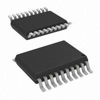
IC, DIGITAL ISOLATOR, 60NS, SSOP-20
Manufacturer
Analog Devices Inc
Series
iCoupler®r
Datasheet
1.EVAL-ADUM3471EBZ.pdf
(32 pages)
Specifications of ADUM3470CRSZ
No. Of Channels
4
Propagation Delay
60ns
Supply Current
33mA
Supply Voltage Range
3V To 3.6V, 4.5V To 5.5V
Digital Ic Case Style
SSOP
No. Of Pins
20
Operating Temperature
-40°C ~ 105°C
Inputs - Side 1/side 2
4/0
Number Of Channels
4
Isolation Rating
2500Vrms
Voltage - Supply
3.3V, 5V
Data Rate
25Mbps
Output Type
Logic
Package / Case
20-SSOP (0.200", 5.30mm Width)
Rohs Compliant
Yes
Lead Free Status / RoHS Status
Lead free / RoHS Compliant
Lead Free Status / RoHS Status
Lead free / RoHS Compliant


ADuM3470/ADuM3471/ADuM3472/ADuM3473/ADuM3474
Inductors must be selected based on the value and supply current
needed. Most applications with switching frequencies between
500 kHz and 1 MHz and load transients between 10% and 90%
of full load are stable with the 47 μH inductor value listed in Table 19.
Values as large as 200 μH can be used for power supply applications
with a switching frequency as low as 200 kHz to help stabilize the
output voltage or for improved load transient response (see Figure 30
to Figure 33). Inductors in a small 1212 or 1210 size are listed in
Table 19 with a 47 μH value and a 0.41 A current rating to handle the
majority of applications below a 400 mA load, and with a 100 μH
value and a 0.34 A current rating to handle a load to 300 mA.
Schottky diodes are recommended for their low forward voltage
to reduce losses and their high reverse voltage of up to 40 V to
withstand the peak voltages available in the doubling circuit
shown in Figure 39 and Figure 40.
Table 19. Recommended Components
Part Number
GRM32ER71A476KE15L
GRM32ER71C226KEA8L
GRM31CR71A106KA01L
MBR0540T1-D
LQH3NPN470MM0
ME3220-104KL
PRINTED CIRCUIT BOARD (PCB) LAYOUT
Note that the total lead length between the ends of the low ESR
capacitor and the V
Installing the bypass capacitor with traces more than 2 mm
in length can result in data corruption. See Figure 41 for the
recommended PCB layout.
In applications involving high common-mode transients, take
care to ensure that board coupling across the isolation barrier is
minimized. Furthermore, design the board layout such that
any coupling that does occur equally affects all pins on a given
component side. Failure to ensure this can cause voltage
differentials between pins, exceeding the absolute maximum
ratings specified in Table 10, thereby leading to latch-up and/or
permanent damage.
V
V
V
V
IB
ID
IA
IC/
GND
GND
V
V
/V
/V
/V
V
DDA
DD1
OB
OC
OD
X1
X2
OA
1
1
Figure 41. Recommended PCB Layout
DDx
and GND
Manufacturer
Murata
Murata
Murata
ON Semiconductor
Murata
Coilcraft
x
pins must not exceed 2 mm.
Value
47 μF, 10 V, X7R,
1210
22 μF, 16 V, X7R,
1210
10 μF, 10 V, X7R,
1206
0.5 A, 40 V,
Schottky, SOD-123
47 μH, 0.41 A,
1212
100 μH, 0.34 A,
1210
V
GND
V
FB
V
V
V
V
OC
GND
REG
DD2
OA
OB
OC
OD
/V
/V
/V
/V
2
2
IA
IB
IC
ID
Rev. 0 | Page 28 of 32
The ADuM347x are power devices that dissipate about 1 W of
power when fully loaded and running at maximum speed. Because
it is not possible to apply a heat sink to an isolation device, the
devices primarily depend on heat dissipation into the PCB through
the GND pins. If the devices are used at high ambient temperatures,
care must be taken to provide a thermal path from the GNDx
pins to the PCB ground plane. The board layout shows enlarged
pads for the GNDx pins (Pin 2 and Pin 10) on Side 1 and (Pin 11
and Pin 19) on Side 2. Large diameter vias should be implemented
from the pad to the ground planes and power planes to increase
thermal conductivity and to reduce inductance. Multiple vias in
the thermal pads can significantly reduce temperatures inside
the chip. The dimensions of the expanded pads are left to the
discretion of the designer and the available board space.
THERMAL ANALYSIS
The ADuM347x parts consist of two internal die attached to a
split lead frame with two die attach paddles. For the purposes of
thermal analysis, the die are treated as a thermal unit, with the
highest junction temperature reflected in the θ
The value of θ
mounted on a JEDEC standard, 4-layer board with fine width traces
and still air. Under normal operating conditions, the ADuM347x
devices operate at full load across the full temperature range
without derating the output current. However, following the
recommendations in the Printed Circuit Board (PCB) Layout
section decreases thermal resistance to the PCB, allowing
increased thermal margins in high ambient temperatures. The
ADuM347x has an thermal shutdown circuit that shuts down
the dc-to-dc converter and the outputs of the ADuM347x when
a die temperature of about 160°C is reached. When the die cools
below about 140°C, the ADuM347x dc-to-dc converter and
outputs turn on again.
PROPAGATION DELAY-RELATED PARAMETERS
Propagation delay is a parameter that describes the time it takes
a logic signal to propagate through a component (see Figure 42).
The propagation delay to a logic low output may differ from the
propagation delay to a logic high output.
Pulse width distortion is the maximum difference between these
two propagation delay values and is an indication of how
accurately the input signal timing is preserved.
Channel-to-channel matching refers to the maximum amount
the propagation delay differs between channels within a single
ADuM347x component.
Propagation delay skew refers to the maximum amount the
propagation delay differs between multiple ADuM347x
components operating under the same conditions.
INPUT (V
OUTPUT (V
Ix
)
Ox
)
JA
Figure 42. Propagation Delay Parameters
is based on measurements taken with the parts
t
PLH
t
PHL
50%
JA
from Table 5.
50%
Related parts for ADUM3470CRSZ
Image
Part Number
Description
Manufacturer
Datasheet
Request
R

Part Number:
Description:
±1.7g Dual-Axis IMEMS Accelerometer Evaluation Board
Manufacturer:
Analog Devices Inc
Datasheet:

Part Number:
Description:
Inertial Sensor Evaluation System
Manufacturer:
Analog Devices Inc
Datasheet:
Part Number:
Description:
Manufacturer:
Analog Devices Inc
Datasheet:
Part Number:
Description:
Manufacturer:
Analog Devices Inc
Datasheet:
Part Number:
Description:
Manufacturer:
Analog Devices Inc
Datasheet:
Part Number:
Description:
Manufacturer:
Analog Devices Inc
Datasheet:
Part Number:
Description:
Manufacturer:
Analog Devices Inc
Datasheet:
Part Number:
Description:
Manufacturer:
Analog Devices Inc
Datasheet:
Part Number:
Description:
Manufacturer:
Analog Devices Inc
Datasheet:
Part Number:
Description:
Manufacturer:
Analog Devices Inc
Datasheet:
Part Number:
Description:
Manufacturer:
Analog Devices Inc
Datasheet:
Part Number:
Description:
Manufacturer:
Analog Devices Inc
Datasheet:
Part Number:
Description:
Manufacturer:
Analog Devices Inc
Datasheet: