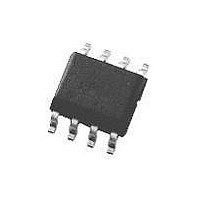
DS90LV018ATM National Semiconductor, DS90LV018ATM Datasheet

DS90LV018ATM
Specifications of DS90LV018ATM
Available stocks
Related parts for DS90LV018ATM
DS90LV018ATM Summary of contents
Page 1
... PCB layout. The DS90LV018A and companion LVDS line driver provide a new alternative to high power PECL/ECL devices for high speed point-to-point interface applications. Connection Diagram SOIC Order Number DS90LV018ATM See NS Package Number M08A Functional Diagram © 2005 National Semiconductor Corporation Features > ...
Page 2
... Absolute Maximum Ratings If Military/Aerospace specified devices are required, please contact the National Semiconductor Sales Office/ Distributors for availability and specifications. Supply Voltage ( Input Voltage ( − Output Voltage (R ) OUT Maximum Package Power Dissipation M Package Derate M Package 8.2 mW/˚C above +25˚C Storage Temperature Range Lead Temperature Range Soldering (4 sec ...
Page 3
Switching Characteristics Note 10 part to part skew, is the differential channel-to-channel skew of any event between devices. This specification applies to devices over the SKD4 recommended operating temperature and voltage ranges, and across process distribution. t Note ...
Page 4
Applications Information offset voltage which is typically +1.2V. The driven signal is centered around this voltage and may shift ± center point. The 1V shifting may be the result of a ground potential difference between the driver’s ground reference and ...
Page 5
... Non-inverting receiver input pin Receiver output pin OUT 8 V Power supply pin, +3. GND Ground pin NC No connection Package Type/ Order Number Number SOP/M08A DS90LV018ATM 10007807 5 < 0.5M, most cables can be made to ± 0.3V Output Low Voltage vs Power Supply Voltage 10007808 www.national.com ...
Page 6
Typical Performance Characteristics Output Short Circuit Current vs Power Supply Voltage Power Supply Current vs Frequency Differential Propagation Delay vs Power Supply Voltage www.national.com (Continued) Differential Transition Voltage vs Power Supply Voltage 10007809 Power Supply Current vs Ambient Temperature 10007811 ...
Page 7
Typical Performance Characteristics Differential Skew vs Power Supply Voltage Differential Propagation Delay vs Differential Input Voltage Transition Time vs Power Supply Voltage (Continued) 10007815 Differential Propagation Delay vs Common-Mode Voltage 10007817 10007819 7 Differential Skew vs Ambient Temperature 10007816 10007818 ...
Page 8
Typical Performance Characteristics Differential Propagation Delay vs Load Differential Propagation Delay vs Load www.national.com (Continued) 10007822 10007821 8 Transition Time vs Load 10007823 Transition Time vs Load 10007824 ...
Page 9
... Tel: 1-800-272-9959 Deutsch Tel: +49 (0) 69 9508 6208 English www.national.com Français Tel: +33 ( 8790 Order Number DS90LV018ATM NS Package Number M08A 2. A critical component is any component of a life support device or system whose failure to perform can be reasonably expected to cause the failure of the life support device or system affect its safety or effectiveness ...


