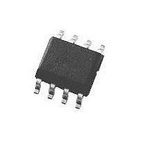
LM555CM National Semiconductor, LM555CM Datasheet - Page 10

LM555CM
Manufacturer Part Number
LM555CM
Description
IC, TIMER, SINGLE, 16V, 8-SOIC
Manufacturer
National Semiconductor
Datasheet
1.LM555CM.pdf
(12 pages)
Specifications of LM555CM
Operating Mode
Astable / Monostable
No. Of Timers
1
Clock External Input
Yes
Supply Voltage Range
4.5V To 16V
Digital Ic Case Style
SOIC
No. Of Pins
8
Operating Temperature Range
0°C To +70°C
Lead Free Status / RoHS Status
Contains lead / RoHS non-compliant
Available stocks
Company
Part Number
Manufacturer
Quantity
Price
Part Number:
LM555CM
Manufacturer:
NS
Quantity:
20 000
Part Number:
LM555CM/NOPB
Manufacturer:
TI/德州仪器
Quantity:
20 000
Part Number:
LM555CMM
Manufacturer:
NS/国半
Quantity:
20 000
Company:
Part Number:
LM555CMM/NOPB
Manufacturer:
AD
Quantity:
5 550
Part Number:
LM555CMX
Manufacturer:
FSC
Quantity:
20 000
Part Number:
LM555CMX NOPB
Manufacturer:
NS/国半
Quantity:
20 000
Company:
Part Number:
LM555CMX/NOPB
Manufacturer:
NS
Quantity:
6 263
www.national.com
Applications Information
V
TIME = 20µs/DIV. Middle Trace: Output 5V/Div.
R
R
R
C = 0.01 µF
50% DUTY CYCLE OSCILLATOR
For a 50% duty cycle, the resistors R
connected as in Figure 14. The time period for the output
high is the same as previous, t
low it is t
Thus the frequency of oscillation is
CC
1
2
E
= 47kΩ
= 100kΩ
= 2.7 kΩ
= 5V
2
=
Bottom Trace: Capacitor Voltage 1V/Div.
Top Trace: Input 3V/Div.
FIGURE 13. Linear Ramp
1
= 0.693 R
A
A
and R
C. For the output
00785117
(Continued)
B
may be
10
Note that this circuit will not oscillate if R
R
down to 1/3 V
ADDITIONAL INFORMATION
Adequate power supply bypassing is necessary to protect
associated circuitry. Minimum recommended is 0.1µF in par-
allel with 1µF electrolytic.
Lower comparator storage time can be as long as 10µs
when pin 2 is driven fully to ground for triggering. This limits
the monostable pulse width to 10µs minimum.
Delay time reset to output is 0.47µs typical. Minimum reset
pulse width must be 0.3µs, typical.
Pin 7 current switches within 30ns of the output (pin 3)
voltage.
A
because the junction of R
FIGURE 14. 50% Duty Cycle Oscillator
CC
and trigger the lower comparator.
A
and R
B
B
cannot bring pin 2
is greater than 1/2
00785118


