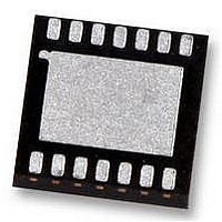
LP3947ISD-51 National Semiconductor, LP3947ISD-51 Datasheet - Page 13

LP3947ISD-51
Manufacturer Part Number
LP3947ISD-51
Description
CHARGER, USB, I2C, POWERWISE, LLP-14
Manufacturer
National Semiconductor
Datasheet
1.LP3947ISD-51.pdf
(14 pages)
Specifications of LP3947ISD-51
Battery Type
Li-Ion
Input Voltage
6V
Battery Charge Voltage
4.2V
Charge Current Max
750mA
Battery Ic Case Style
LLP
No. Of Pins
14
No. Of Series Cells
1
Operating Temperature Range
-40°C
Lead Free Status / RoHS Status
Lead free / RoHS Compliant
Available stocks
Company
Part Number
Manufacturer
Quantity
Price
Company:
Part Number:
LP3947ISD-51/NOPB
Manufacturer:
SONY
Quantity:
6 242
Application Notes
w = write (sda = “0”)
r = read (sda = “1”)
ack = acknowledge (sda pulled low by either master or slave)
Nack = No Acknowledge
rs = repeated start
THERMAL PERFORMANCE OF LLP PACKAGE
The LP3947 is a monolithic device with an integrated pass
transistor. To enhance the power dissipation performance,
the Leadless Lead frame Package, or LLP, is used. The LLP
package is designed for improved thermal performance be-
cause of the exposed die attach pad at the bottom center of
the package. It brings advantage to thermal performance by
creating a very direct path for thermal dissipation. Compared
to the traditional leaded packages where the die attach pad
is embedded inside the mold compound, the LLP reduces a
layer of thermal path.
The thermal advantage of the LLP package is fully realized
only when the exposed die attach pad is soldered down to a
thermal land on the PCB board and thermal vias are planted
underneath the thermal land. Based on a LLP thermal mea-
surement, junction to ambient thermal resistance (θ
be improved by as much as two times if a LLP is soldered on
the board with thermal land and thermal vias than if not.
An example of how to calculate for LLP thermal performance
is shown below:
By substituting 37˚C/W for θ
the maximum power dissipation allowed from the chip is
1.48W. If V
CHG-IN
is at 5.0V and a 3.0V battery is being
JA
, 125˚C for T
(Continued)
FIGURE 8. LP3947 (Slave) Register Read
J
and 70˚C for T
JA
) can
A
,
13
charged, then 740 mA of I
More power can be dissipated at ambient temperatures
below 70˚C. Less power can be dissipated at ambient tem-
peratures above 70˚C. The maximum power dissipation for
operation can be increased by 27 mW for each degree below
70˚C, and it must be de-rated by 27 mW for each degree
above 70˚C.
LAYOUT CONSIDERATION
The LP3947 has an exposed die attach pad located at the
bottom center of the LLP package. It is imperative to create
a thermal land on the PCB board when designing a PCB
layout for the LLP package. The thermal land helps to con-
duct heat away from the die, and the land should be the
same dimension as the exposed pad on the bottom of the
LLP (1:1 ratio). In addition, thermal vias should be added
inside the thermal land to conduct more heat away from the
surface of the PCB to the ground plane. Typical pitch and
outer diameter for these thermal vias are 1.27 mm and 0.33
mm respectively. Typical copper via barrel plating is 1oz
although thicker copper may be used to improve thermal
performance. The LP3947 bottom pad is connected to
ground. Therefore, the thermal land and vias on the PCB
board need to be connected to ground.
For more information on board layout techniques, refer to
Application Note 1187 “Leadless Leadframe Package
(LLP).” The application note also discusses package han-
dling, solder stencil, and assembly.
CHG
can safely charge the battery.
www.national.com
20111013


