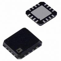
ADA4859-3ACPZ-R2 Analog Devices Inc, ADA4859-3ACPZ-R2 Datasheet - Page 6

ADA4859-3ACPZ-R2
Manufacturer Part Number
ADA4859-3ACPZ-R2
Description
IC, VIDEO AMPLIFIER, TRI, 195MHZ LFCSP16
Manufacturer
Analog Devices Inc
Datasheet
1.ADA4859-3ACPZ-R7.pdf
(16 pages)
Specifications of ADA4859-3ACPZ-R2
Gain Bandwidth
195MHz
Supply Voltage Range
3V To 5.5V
Slew Rate
740V/µs
No. Of Amplifiers
3
Output Current
19mA
Amplifier Output
Single Ended
Operating Temperature Range
-40°C To +105°C
Applications
Current Feedback
Number Of Circuits
3
-3db Bandwidth
265MHz
Current - Supply
17mA
Current - Output / Channel
19mA
Voltage - Supply, Single/dual (±)
3 V ~ 5.5 V
Mounting Type
Surface Mount
Package / Case
16-VQFN, CSP Exposed Pad
Rohs Compliant
Yes
Lead Free Status / RoHS Status
Lead free / RoHS Compliant
ADA4859-3
PIN CONFIGURATION AND FUNCTION DESCRIPTIONS
Table 4. Pin Function Descriptions
Pin No.
1
2
3
4
5
6
7
8
9
10
11
12
13
14
15
16
17 (EPAD)
Mnemonic
+V
C1_a
C1_b
CPO
+V
+IN3
−IN3
OUT3
PD
OUT2
−IN2
+IN2
NC
+IN1
−IN1
OUT1
Exposed Pad (EPAD)
S
S
NOTES
1. NC = NO CONNECT.
2. EXPOSED PAD, CONNECT TO GROUND.
C1_b
C1_a
CPO
+V
S
1
2
3
4
Figure 3. Pin Configuration
CHARGE
PUMP
16
Rev. 0 | Page 6 of 16
5
ADA4859-3
(Not to Scale)
TOP VIEW
Description
Positive Supply for Charge Pump.
Charge Pump Capacitor Side a.
Charge Pump Capacitor Side b.
Charge Pump Output.
Positive Supply.
Noninverting Input 3.
Inverting Input 3.
Output 3.
Power Down.
Output 2.
Inverting Input 2.
Noninverting Input 2.
No Connect.
Noninverting Input 1.
Inverting Input 1.
Output 1.
The exposed pad must be connected to the ground plane.
15
6
14
7
13
8
12 +IN2
11 –IN2
10 OUT2
9
PD


