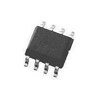
LMH6672MA National Semiconductor, LMH6672MA Datasheet - Page 11

LMH6672MA
Manufacturer Part Number
LMH6672MA
Description
IC, OP-AMP, 90MHZ, 135V/µs, SOIC-8
Manufacturer
National Semiconductor
Datasheet
1.LMH6672MRNOPB.pdf
(14 pages)
Specifications of LMH6672MA
Op Amp Type
High Speed
No. Of Amplifiers
2
Bandwidth
90MHz
Slew Rate
135V/µs
Supply Voltage Range
± 2.5V To ± 6.5V
Amplifier Case Style
SOIC
No. Of Pins
8
Lead Free Status / RoHS Status
Contains lead / RoHS non-compliant
Lead Free Status / RoHS Status
Contains lead / RoHS non-compliant
Available stocks
Company
Part Number
Manufacturer
Quantity
Price
Company:
Part Number:
LMH6672MA
Manufacturer:
NS
Quantity:
5 000
Part Number:
LMH6672MA
Manufacturer:
NS/国半
Quantity:
20 000
Company:
Part Number:
LMH6672MAX
Manufacturer:
PH
Quantity:
5 878
Part Number:
LMH6672MAX
Manufacturer:
NS/国半
Quantity:
20 000
Company:
Part Number:
LMH6672MAX/NOPB
Manufacturer:
NS
Quantity:
12 500
Company:
Part Number:
LMH6672MAX/NOPB
Manufacturer:
NS
Quantity:
6 231
Company:
Part Number:
LMH6672MAXNOPB
Manufacturer:
NSC
Quantity:
7 121
Application Notes
THERMAL MANAGEMENT
The LMH6672 is a high-speed, high power, dual operational
amplifier with a very high slew rate and very low distortion.
For ease of use, it uses conventional voltage feedback.
These characteristics make the LMH6672 ideal for applica-
tions where driving low impedances of 25-100Ω such as
xDSL and active filters.
A class AB output stage allows the LMH6672 to deliver high
currents to low impedance loads with low distortion while
consuming low quiescent supply current. For most op-amps,
class AB topology means that internal power dissipation is
rarely an issue, even with the trend to smaller surface mount
packages. However, the LMH6672 has been designed for
applications where high levels of power dissipation may be
encountered.
Several factors contribute to power dissipation and conse-
quently higher junction temperatures. These factors need to
be well understood if the LMH6672 is to perform to specifi-
cations in all applications. This section will examine the
typical application that is shown on the front page of this data
sheet as an example. (Figure 1) Because both amplifiers are
in a single package, the calculations will for the total power
dissipated by both amplifiers.
There are two separate contributors to the internal power
dissipation:
1. The product of the supply voltage and the quiescent
2. The additional power dissipated while delivering power
The first of these components appears easy to calculate
simply by inspecting the data sheet. The typical quiescent
supply current for this part is 7.2 mA per amplifier, therefore,
with a
P
With a thermal resistance of 172˚C/W for the SOIC package,
this level of internal power dissipation will result in a junction
temperature (T
D
(V
= V
current when no signal is being delivered to the external
load.
to the external load.
S
= V
±
S
6 volt supply, the total power dissipation is:
x 2 x l
CC
+ V
J
Q
) of 30˚C above ambient.
EE
= 12 x (14.4x10
)
-3
) = 173 mW
e
n
& i
n
vs. Frequency, V
11
Using the worst-case maximum supply current of 18 mA and
an ambient of 85˚C, a similar calculation results in a power
dissipation of 216 mW, or a T
This is approaching the maximum allowed T
fore a signal is applied. Fortunately, in normal operation, this
term is reduced, for reasons that will soon be explained.
The second contributor to high T
internally when power is delivered to the external load. This
cause of temperature rise is more difficult to calculate, even
when the actual operating conditions are known.
To maintain low distortion, in a Class AB output stage, an idle
current, I
when there is little or no output signal. In the LMH6672,
about 4.8 mA of the total quiescent supply current of 14.4 mA
flows through the output stages.
Under normal large signal conditions, as the output voltage
swings positive, one transistor of the output pair will conduct
the load current, while the other transistor shuts off, and
dissipates no power. During the negative signal swing this
situation is reversed, with the lower transistor sinking the
load current while the upper transistor is cut off. The current
in each transistor will approximate a half wave rectified
version of the total load current.
Because the output stage idle current is now routed into the
load, 4.8 mA can be subtracted from the quiescent supply
current when calculating the quiescent power when the out-
put is driving a load.
The power dissipation caused by driving a load in a DSL
application, using a 1:2 turns ratio transformer driving 20
mW into the subscriber line and 20 mW into the back termi-
nation resistors, can be calculated as follows:
P
P
P
P
tors
P
At full specified power, P
x I
In this application, V
I
idle current.
Q
S
DRIVER
DRIVER
TOT
TERM
LINE
I
S
= the LMH6672 quiescent current minus the output stage
= 5V and 12V
S
.
= I
is the total power drawn from the power supply
is the power sent into the subscriber line
is the power dissipated in the back termination resis-
Q
is the LMH6672 power dissipation
= P
Q
+ A
, is maintained through the output transistors
TOT
VG
20016610
|I
– (P
OUT
S
TERM
|.
= 12V.
TERM
+ P
J
= P
LINE
of 122˚C.
J
LINE
) where
is the power dissipated
= 20 mW, P
J
of 150˚C be-
www.national.com
TOT
= V
S


