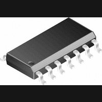
LMH6644MA National Semiconductor, LMH6644MA Datasheet - Page 17

LMH6644MA
Manufacturer Part Number
LMH6644MA
Description
IC, OP-AMP, 130MHZ, 135V/µs, SOIC-14
Manufacturer
National Semiconductor
Datasheet
1.LMH6644MA.pdf
(22 pages)
Specifications of LMH6644MA
Op Amp Type
Low Power
No. Of Amplifiers
1
Bandwidth
130MHz
Slew Rate
135V/µs
Supply Voltage Range
2.7V To 12.8V
Amplifier Case Style
SOIC
No. Of Pins
14
Lead Free Status / RoHS Status
Contains lead / RoHS non-compliant
Available stocks
Company
Part Number
Manufacturer
Quantity
Price
Part Number:
LMH6644MA
Manufacturer:
NS/国半
Quantity:
20 000
Part Number:
LMH6644MAX
Manufacturer:
NS/国半
Quantity:
20 000
Company:
Part Number:
LMH6644MAX/NOPB
Manufacturer:
NS
Quantity:
11 376
SINGLE SUPPLY, LOW POWER PHOTODIODE
AMPLIFIER
The circuit shown in
from a photo-diode into a voltage output. In this circuit, the
emphasis is on achieving high bandwidth and the tran-
simpedance gain setting is kept relatively low. Because of its
high slew rate limit and high speed, the LMH664X family lends
itself well to such an application.
This circuit achieves approximately 1V/mA of tran-
simpedance gain and capable of handling up to 1mA
the photodiode. Q1, in a common base configuration, isolates
the high capacitance of the photodiode (C
input in order to maximize speed. Input is AC coupled through
C1 to ease biasing and allow single supply operation. With 5V
single supply, the device input/output is shifted to near half
supply using a voltage divider from V
does not have any voltage swing and the Miller effect is min-
imized. D1, tied to Q1 base, is for temperature compensation
of Q1’s bias point. Q1 collector current was set to be large
enough to handle the peak-to-peak photodiode excitation and
not too large to shift the U1 output too far from mid-supply.
No matter how low an R
order to stabilize the circuit. The reason for this is that the Op
Figure 3
f
is selected, there is a need for C
is used to amplify the current
CC
FIGURE 3. Single Supply Photodiode I-V Converter
. Note that Q1 collector
d
) from the Op Amp
pp
from
f
in
17
Amp input capacitance and Q1 equivalent collector capaci-
tance together (C
signal fed back to the inverting node. C
in the feedback path counter-acting the effect of the C
acting to stabilized the circuit. By proper selection of C
that the Op Amp open loop gain is equal to the inverse of the
feedback factor at that frequency, the response is optimized
with a theoretical 45° phase margin.
where GBWP is the Gain Bandwidth Product of the Op Amp
Optimized as such, the I-V converter will have a theoretical
pole, f
With Op Amp input capacitance of 3pF and an estimate for
Q1 output capacitance of about 3pF as well, C
the typical performance plots, LMH6642/6643 family GBWP
is approximately 57MHz. Therefore, with R
tion 1 and 2 above.
C
f
=
∼
p
4.1pF, and f
, at:
IN
p
) will cause additional phase shift to the
= 39MHz
f
will function as a zero
f
= 1k, from Equa-
IN
20018564
= 6pF. From
www.national.com
IN
f
such
and
(1)
(2)


