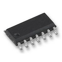
LMC660CM National Semiconductor, LMC660CM Datasheet - Page 6

LMC660CM
Manufacturer Part Number
LMC660CM
Description
OP AMP, QUAD CMOS, SMD, SOIC14, 660
Manufacturer
National Semiconductor
Datasheet
1.LMC660CM.pdf
(14 pages)
Specifications of LMC660CM
Op Amp Type
Low Input Bias
No. Of Amplifiers
4
Bandwidth
0.5MHz
Slew Rate
1.1V/µs
Supply Voltage Range
4.75V To 15.5V
Amplifier Case Style
SOIC
No. Of Pins
14
Operating Temperature
RoHS Compliant
Available stocks
Company
Part Number
Manufacturer
Quantity
Price
Part Number:
LMC660CM
Manufacturer:
NS/国半
Quantity:
20 000
Company:
Part Number:
LMC660CM/NOPB
Manufacturer:
TI
Quantity:
9 289
Company:
Part Number:
LMC660CMD-734
Manufacturer:
NS
Quantity:
351
Part Number:
LMC660CMX
Manufacturer:
TI/德州仪器
Quantity:
20 000
Company:
Part Number:
LMC660CMX/NOPB
Manufacturer:
TI
Quantity:
14 390
Part Number:
LMC660CMX/NOPB
Manufacturer:
TI/德州仪器
Quantity:
20 000
www.national.com
Typical Performance Characteristics
Note: Avoid resistive loads of less than 500Ω, as they may cause instability.
Application Hints
AMPLIFIER TOPOLOGY
The topology chosen for the LMC660, shown in Figure 1, is
unconventional (compared to general-purpose op amps) in
that the traditional unity-gain buffer output stage is not used;
instead, the output is taken directly from the output of the
integrator, to allow rail-to-rail output swing. Since the buffer
traditionally delivers the power to the load, while maintaining
high op amp gain and stability, and must withstand shorts to
either rail, these tasks now fall to the integrator.
As a result of these demands, the integrator is a compound
affair with an embedded gain stage that is doubly fed forward
(via C
driver. In addition, the output portion of the integrator is a
push-pull configuration for delivering heavy loads. While
sinking current the whole amplifier path consists of three
gain stages with one stage fed forward, whereas while
sourcing the path contains four gain stages with two fed
forward.
f
and Cff) by a dedicated unity-gain compensation
Frequency Response
vs Capacitive Load
Capacitive Load
Stability vs
00876734
00876732
V
6
S
=
The large signal voltage gain while sourcing is comparable
to traditional bipolar op amps, even with a 600Ω load. The
gain while sinking is higher than most CMOS op amps, due
to the additional gain stage; however, under heavy load
(600Ω) the gain will be reduced as indicated in the Electrical
Characteristics.
±
FIGURE 1. LMC660 Circuit Topology (Each Amplifier)
7.5V, T
A
= 25˚C unless otherwise specified (Continued)
Non-Inverting Large Signal
Pulse Response
Capacitive Load
Stability vs
00876735
00876733
00876704


