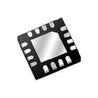
MMA6270QR2 Freescale Semiconductor, MMA6270QR2 Datasheet - Page 5

MMA6270QR2
Manufacturer Part Number
MMA6270QR2
Description
SENSOR ACCEL XY-AX +/-1.5G 16QFN
Manufacturer
Freescale Semiconductor
Datasheet
1.KIT3109MMA6270QE.pdf
(12 pages)
Specifications of MMA6270QR2
Axis
X, Y
Acceleration Range
±1.5g, 2g, 4g, 6g (Config)
Sensitivity
800mV/g, 600mV/g, 300mV/g, 200mV/g
Voltage - Supply
2.2 V ~ 3.6 V
Output Type
Analog
Bandwidth
350Hz
Mounting Type
Surface Mount
Package / Case
16-QFN
Package Type
QFN EP
Operating Supply Voltage (min)
2.2V
Operating Supply Voltage (typ)
3.3V
Operating Supply Voltage (max)
3.6V
Operating Temperature (min)
-40C
Operating Temperature (max)
105C
Operating Temperature Classification
Industrial
Product Depth (mm)
6mm
Product Height (mm)
1.45mm
Product Length (mm)
6mm
Mounting
Surface Mount
Pin Count
16
Sensing Axis
X, Y
Acceleration
1.5 g, 2 g, 4 g, 6 g
Maximum Operating Temperature
+ 105 C
Minimum Operating Temperature
- 40 C
Mounting Style
SMD/SMT
For Use With
RD3152MMA7260Q - BOARD REF 3-AXIS ACCELEROMETER
Lead Free Status / RoHS Status
Lead free / RoHS Compliant
Interface
-
Lead Free Status / Rohs Status
Compliant
Other names
MMA6270QR2
MMA6270QR2TR
MMA6270QR2TR
Pin Descriptions
Table 4. Pin Descriptions
Sensors
Freescale Semiconductor
Pin No.
8 - 11
5 - 7
12
13
14
15
16
1
2
3
4
V
Figure 5. Accelerometer with Recommended
DD
0.1 μF
g-Select1
g-Select2
Sleep Mode
Logic
Input
Logic
Inputs
Pin Name
g-Select1
g-Select2
V
V
Figure 4. Pinout Description
Y
X
DD
V
SS
V
N/C
N/C
N/C
N/C
OUT
OUT
DD
SS
Connection Diagram
2
4
3
1
12
3
4
1
2
g-Select1
g-Select2
Sleep Mode
V
V
16
5
DD
SS
Logic input pin to select g level.
Logic input pin to select g level.
Power Supply Input
Power Supply Ground
No internal connection.
Leave unconnected.
Unused for factory trim.
Leave unconnected.
Logic input pin to enable product or
Sleep Mode.
No internal connection.
Leave unconnected
Y direction output voltage.
X direction output voltage.
No internal connection.
Leave unconnected.
Top View
MMA6270QT
15
6
14 13
7
Y
X
OUT
OUT
8
Description
11
10
14
15
12
9
0.1 μF
0.1 μF
N/C
Sleep Mode
N/C
N/C
1 kΩ
1 kΩ
BASIC CONNECTIONS
PCB Layout
NOTES:
Figure 6. Recommended PCB Layout for Interfacing
1. Verify V
2. Physical coupling distance of the accelerometer to
3. The flag underneath the package is internally
4. Place a ground plane beneath the accelerometer to
5. Use an RC filter with 1.0 kW and 0.1 µF on the
6. PCB layout of power and ground should not couple
7. Accelerometer and microcontroller should not be a
8. A/D sampling rate and any external power supply
9. PCB layout should not run traces or vias under the
Sleep Mode
g-Select1
g-Select2
0.1 ms as measured on the device at the V
Rise times greater than this most likely will prevent
start up operation.
the microcontroller should be minimal.
connected to ground. It is not recommended for the
flag to be soldered down.
reduce noise, the ground plane should be attached to
all of the open ended terminals shown in
outputs of the accelerometer to minimize clock noise
(from the switched capacitor filter circuit).
power supply noise.
high current path.
switching frequency should be selected such that
they do not interfere with the internal accelerometer
sampling frequency (11 kHz for the sampling
frequency). This will prevent aliasing errors.
QFN part. This could lead to ground shorting to the
accelerometer flag.
X
Y
V
V
OUT
OUT
DD
Accelerometer to Microcontroller
SS
POWER SUPPLY
DD
C
line has the ability to reach 2.2 V in <
R
R
C
C
C
C
P2
A/D
A/D
V
P0
P1
RH
IN
IN
MMA6270QT
Figure
DD
V
V
DD
SS
pin.
6.
C
C
5


