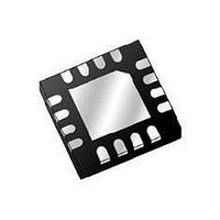
MMA5224WR2 Freescale Semiconductor, MMA5224WR2 Datasheet - Page 31

MMA5224WR2
Manufacturer Part Number
MMA5224WR2
Description
IC ACCELER 240G X-AXIS 16QFN
Manufacturer
Freescale Semiconductor
Datasheet
1.MMA5206WR2.pdf
(63 pages)
Specifications of MMA5224WR2
Sensing Axis
X
Acceleration
240 g
Sensitivity
0.5 g/LSB
Package / Case
QFN-16
Supply Voltage (max)
25 V
Supply Current
4 mA to 8 mA
Maximum Operating Temperature
+ 125 C
Minimum Operating Temperature
- 40 C
Mounting Style
SMD/SMT
Lead Free Status / RoHS Status
Lead free / RoHS Compliant
3.5.3.4
continuously monitored against the offset limits specified in
exceeds the limits, and to count down if the output is within the limits. The output of the counter is compared against the count
limit OFFMON
max counter value is reached (OFFMON
Phase 3.
3.5.3.5
signal processing chain is delayed one sample time. On detection of a sync pulse the transmitted data is interpolated from the
2 previous samples, resulting in a latency of one sample time, and a maximum signal jitter of ±1/16 of a sample time. Reference
Section 4.5
3.5.3.6
device.
3.5.3.7
register. When the PCM function is enabled, a 4 MHz Pulse Code Modulated signal proportional to the upper 9 bits of the 10-bit
acceleration response is output onto the PCM pin. The PCM output is intended for test use only.
D25
Sensors
Freescale Semiconductor
The device includes an offset monitor circuit. The output of the single pole low pass filter in the offset cancellation block is
The device includes 16 to 1 linear data interpolation to minimize the system sample jitter. Each result produced by the digital
The 26 bit digital output from the DSP is clipped and scaled to a 10-bit or 8-bit word which spans the acceleration range of the
The device provides the option for a PCM output function. The PCM output is activated if the PCM bit is set in the DEVCFG2
Over Range
10-bit Data Word
8-bit Data Word
D24
Figure 22
Sample updated every 16μS
for more information regarding interpolation and data latency.
Output Scaling
Section 3.5.3.6
D23
Offset Monitor
CNTLIMIT
Data Interpolation
Output Scaling
PCM Output Function
D[21:13]
shows the method used to establish the output acceleration data word from the 26-bit DSP output.
D22
. If the counter exceeds the limit, the OFF_B flag in the SC register is cleared. The counter rails once the
D21
D21
D21
9
D20
D20
D20
D19
D19
D19
Figure 23. PCM Output Function Block Diagram
A
B
CNTSIZE
Figure 22. 10-Bit Output Scaling Diagram
f
D18
D18
D18
9 Bit ADDER
CLK
Signal
= 4 MHz
D17
D17
D17
CARRY
). The offset monitor is disabled during Initialization Phase1, Phase 2, and
SUM
D16
D16
D16
9
Section
D15
D15
D15
9
D14
D14
D14
2.4. An up/down counter is employed to count up If the output
D
D13
D13
D
CLK
D
CLK
D
CLK
D
CLK
D
CLK
D
CLK
D
FF
CLK
D
CLK
FF
FF
CLK
D12
D12
FF
FF
FF
FF
FF
Q
Q
FF
Q
Q
Q
Q
Q
Q
D11
Q
Q
Q
Q
Q
Q
Q
Q
Noise
Q
Q
D10
Using Rounding
D9
Using Rounding
D8
...
Margin
D2
MMA52xxWR
PCM
D1
D0
31


