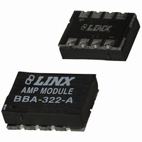
BBA-322-A Linx Technologies Inc, BBA-322-A Datasheet

MODULE RF AMP HI-GAIN BROADBAND

BBA-322-A

Manufacturer Part Number
BBA-322-A
Description
MODULE RF AMP HI-GAIN BROADBAND
Manufacturer
Linx Technologies Inc
Type
RF Amplifierr
Datasheet

Specifications of BBA-322-A

P1db
11.2dBm
Noise Figure
3.8dBm
Current - Supply
35mA ~ 60mA
Frequency
0Hz ~ 3GHz
Gain
20dB
Package / Case
Module
Rf Type
General Purpose
Test Frequency
2GHz
Voltage - Supply
4.8 V ~ 5.2 V
Operating Frequency
3000 MHz
Operating Supply Voltage
4.8 V to 5.2 V
Supply Current
35 mA
Maximum Operating Temperature
+ 85 C
Minimum Operating Temperature
- 40 C
Lead Free Status / RoHS Status
Lead free / RoHS Compliant
Lead Free Status / RoHS Status
Lead free / RoHS Compliant, Lead free / RoHS Compliant
DESCRIPTION
The BBA Series is a family of low-cost high-
performance broadband RF amplifiers.
modules are ideally suited to a wide range of
amplification
including extending the range of Linx’s own RF
modules (where legally appropriate). Housed in
a compact SMD package, the hybrid amps are
matched to 50Ω source and load impedances.
The modules utilize a GaHBT gain stage, which
yields high gain and IP3, excellent flatness, and
low noise. The BBA-322-A is the high gain
model and is suitable for the LNA stage of many
receivers. This extra gain stage on the front end
of a receiver can improve the sensitivity and
provide a greater range for the product. The BBA-519-A is the high power model and
is suitable for the final gain stage in a transmitter. This amplifier can boost the output
power of a transmitter to much higher levels and provide a significant increase in
range (where legally appropriate).
BBA SERIES FEATURES
BBA-322-A FEATURES
APPLICATIONS INCLUDE
Prematched for 50Ω impedance
No external RF components
High gain
3.8dB noise figure
DC-3GHz broadband operation
+20dB small signal gain at
Up to +10dB (10mW) linear
TX / RX Range Enhancement
IF or RF Buffering
Driver or Final Stage for PA
General Purpose Gain Blocks
required
900MHz
output power
BBA SERIES RF AMPLIFIER DATA GUIDE
WIRELESS MADE SIMPLE
and
buffering
applications,
®
BBA-322-A
BBA-519-A
BBA-519-A FEATURES
The
PART #
BBA-322-A
BBA-519-A
Amplifiers are supplied in tubes of 50 pcs.
ORDERING INFORMATION
High output
4.8dB noise figure
10MHz-3GHz broadband
+18dB small signal gain at
Up to +17dB (50mW) linear
Exceptional gain flatness
Compact SMD package
Operates from a single supply
operation
900MHz
output power
Figure 1: BBA Package Dimensions
0.130"
0.360"
Typ.
DESCRIPTION
High Gain RF Amplifier
High Power RF Amplifier
AMP MODULE
BBA-519-A
LOT 0100
0.500"
Revised 1/28/08

Related parts for BBA-322-A

BBA-322-A Summary of contents

Page 1

... The modules utilize a GaHBT gain stage, which yields high gain and IP3, excellent flatness, and low noise. The BBA-322-A is the high gain model and is suitable for the LNA stage of many receivers. This extra gain stage on the front end ...

Page 2

... BBA-322-A ELECTRICAL SPECIFICATIONS Parameter Designation Min. POWER SUPPLY Operating Voltage V 4.8 CC Supply Current I – CC AMPLIFIER SECTION Frequency Range Gain: – -50 @ 100MHz – @ 1,000MHz – @ 2,000MHz – @ 3,000MHz – Gain Ripple – – Noise Figure – – Input VSWR – – Output VSWR – ...

Page 3

... They are self-contained with 50Ω input and output impedances and require only one external DC biasing resistor to operate as specified. The BBA-322-A is the high gain model and is suitable for the LNA stage of many receivers. This extra gain stage on the front end of a receiver can improve the sensitivity and provide a greater range for the product ...

Page 4

... TX DATA TXM-xxx-ES GND In this circuit, the BBA-519-A amplifies the output of the ES Series transmitter. The transmitter operates on 3V while the amplifier requires 5V 270Ω resistor is used to drop the 5V supply to 3V for the transmitter. This configuration would result times increase in system range. Note ...

Page 5

BOARD LAYOUT GUIDELINES If you are at all familiar with RF devices, you may be concerned about specialized board layout requirements. Fortunately, because of the care taken by Linx in designing the modules, integrating them is very straightforward. Despite this ...

Page 6

PAD LAYOUT The following pad layout diagram is designed to facilitate both hand and automated assembly. 0.065" 0.340" 0.100" Figure 9: Recommended PCB Layout PRODUCTION GUIDELINES The modules are housed in a hybrid SMD package that supports hand or automated ...

Page 7

WIRELESS MADE SIMPLE U.S. CORPORATE HEADQUARTERS LINX TECHNOLOGIES, INC. 159 ORT LANE MERLIN, OR 97532 PHONE: (541) 471-6256 FAX: (541) 471-6251 www.linxtechnologies.com Disclaimer Linx Technologies is continually striving to improve the quality and function of its products. For this ...

Related keywords