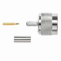
73050 Pomona Electronics, 73050 Datasheet - Page 2
73050
Manufacturer Part Number
73050
Description
CONN PLUG N STR CRIMP RG58, 141
Manufacturer
Pomona Electronics
Series
N Typer
Type
N Type Plugr
Specifications of 73050
Connector Type
Plug, Male Pins
Impedance
50 Ohm
Connector Style
N Type
Contact Termination
Crimp, Single
Mounting Type
Free Hanging (In-Line)
Fastening Type
Threaded
Cable Group
RG-58, 141
Frequency - Max
6GHz
Frequency-max
6GHz
Body Style
Straight Plug
Coaxial Termination
Crimp
Rg Cable Type
RG-58, 141
Contact Material
Brass
Contact Plating
Gold
Frequency Max
6GHz
Product
Connector
Rf Series
N
Gender
Plug
Polarity
Normal
Shell Plating
Nickel
Termination Style
Crimp
Cable Type
RG/U 58, 141
Housing Material
Brass
Maximum Frequency
6 GHz
Angle
Straight
Finish, Housing
Nickel Plated
Material, Contact
Brass
Material, Dielectric
PTFE
Material, Housing
Brass
Mating Type
Bayonet
Primary Type
N
Voltage, Rating
1500 V
Frequency Range
DCââ¬â6 GHz
Insulation Reistance
≤5000 MΩ
Dielectric Withstand Voltage
1500 V
Vswr
≤1.5 V
Number Of Insertions
500 Cycles MinimumFeatures
Connector Accepts Cable Types Rg/u
58, 141
Lead Free Status / RoHS Status
Lead free / RoHS Compliant
Features
-
Color
-
Lead Free Status / Rohs Status
Lead free / RoHS Compliant


BV
∆ΒV
R
V
∆V
I
I
gfs
Q
Q
Q
R
t
t
t
t
C
C
C
E
I
I
I
V
t
Q
Static @ T
Avalanche Characteristics
Diode Characteristics
DSS
GSS
d(on)
r
d(off)
f
AR
S
SM
rr
2
GS(th)
AS
SD
DS(on)
G
iss
oss
rss
g
sw
oss
rr
Q
Q
Q
Q
GS(th)
DSS
gs1
gs2
gd
godr
DSS
/∆T
/∆T
J
J
J
Drain-to-Source Breakdown Voltage
Breakdown Voltage Temp. Coefficient
Static Drain-to-Source On-Resistance
Gate Threshold Voltage
Gate Threshold Voltage Coefficient
Drain-to-Source Leakage Current
Gate-to-Source Forward Leakage
Gate-to-Source Reverse Leakage
Forward Transconductance
Total Gate Charge
Pre-Vth Gate-to-Source Charge
Post-Vth Gate-to-Source Charge
Gate-to-Drain Charge
Gate Charge Overdrive
Switch Charge (Q
Output Charge
Gate Resistance
Turn-On Delay Time
Rise Time
Turn-Off Delay Time
Fall Time
Input Capacitance
Output Capacitance
Reverse Transfer Capacitance
Single Pulse Avalanche Energy
Avalanche Current
Continuous Source Current
(Body Diode)
Pulsed Source Current
(Body Diode)
Diode Forward Voltage
Reverse Recovery Time
Reverse Recovery Charge
= 25°C (unless otherwise specified)
Parameter
Parameter
Ù
Parameter
gs2
Ù
+ Q
gd
)
Min. Typ. Max. Units
Min. Typ. Max. Units
–––
–––
–––
–––
–––
–––
–––
–––
–––
110
–––
–––
–––
–––
–––
–––
–––
–––
–––
–––
–––
–––
–––
–––
–––
–––
–––
–––
–––
–––
1.6
20
6580
2070
0.60
-4.1
–––
–––
–––
–––
–––
–––
–––
–––
840
–––
–––
–––
1.8
1.2
4.4
12
47
14
15
14
19
30
23
95
25
10
32
26
Typ.
-100
0.65
–––
––– mV/°C
––– mV/°C
500
100
–––
–––
–––
–––
–––
–––
–––
–––
–––
–––
–––
–––
–––
–––
–––
–––
200
260
2.5
1.8
2.5
1.4
1.5
71
48
39
5
mΩ
mA
mA
nC
nC
nC
µA
nA
pF
ns
ns
Ω
V
V
S
A
V
V
Reference to 25°C, I
V
V
V
I
V
V
V
V
V
V
V
V
I
See Fig. 17
V
V
I
Clamped Inductive Load
V
V
ƒ = 1.0MHz
MOSFET symbol
showing the
integral reverse
p-n junction diode.
T
T
di/dt = 100A/µs
D
D
D
GS
GS
GS
DS
DS
DS
DS
GS
GS
DS
DS
GS
DS
DD
GS
DS
J
J
= 10mA, reference to 25°C
= 17A
= 26A
= 25°C, I
= 25°C, I
= 0V, I
= 4.5V, I
= 10V, I
= V
= 20V, V
= 16V, V
= 16V, V
= 12V
= -12V
= 10V, I
= 10V
= 4.5V
= 10V, V
= 16V, V
= 0V
= 10V
GS
Max.
230
, I
26
D
Conditions
Conditions
D
S
F
D
D
= 1.0mA
D
GS
GS
GS
GS
GS
= 250µA
= 25A
= 25A, V
= 15A
= 26A
= 12A
e
= 0V
= 0V
= 0V, T
= 0V
= 4.5V
www.irf.com
D
e
e
= 10mA
Ãe
GS
G
J
= 125°C
= 0V
Units
mJ
A
e
D
S
Related parts for 73050
Image
Part Number
Description
Manufacturer
Datasheet
Request
R

Part Number:
Description:
ANTI STATIC FIELD SERVICE KIT
Manufacturer:
Pomona Electronics
Datasheet:

Part Number:
Description:
DOUBLE BANANA PLUG W/BIND POSTS
Manufacturer:
Pomona Electronics
Datasheet:

Part Number:
Description:
EMF SPADE LUG TO BANANA JACK 2PC
Manufacturer:
Pomona Electronics
Datasheet:

Part Number:
Description:
ADAPTER BINDING POST-WE310 PLUG
Manufacturer:
Pomona Electronics
Datasheet:

Part Number:
Description:
MINI BANANA JACK W/TURRET 1=10PC
Manufacturer:
Pomona Electronics
Datasheet:

Part Number:
Description:
MINI BANANA PLUG #4-40X.480"
Manufacturer:
Pomona Electronics
Datasheet:

Part Number:
Description:
ADAPTER BNC FMALE-STD PHONE PLUG
Manufacturer:
Pomona Electronics
Datasheet:

Part Number:
Description:
CONN BNC MALE 50 OHM RG174
Manufacturer:
Pomona Electronics
Datasheet:

Part Number:
Description:
CONN SMA PLUG RG174,179,187 MALE
Manufacturer:
Pomona Electronics
Datasheet:

Part Number:
Description:
RCPT BULKHD TRIAX BNC 3LUG FMALE
Manufacturer:
Pomona Electronics
Datasheet:

Part Number:
Description:
PANEL BNC FEMALE-BNC FEMALE
Manufacturer:
Pomona Electronics
Datasheet:

Part Number:
Description:
ADT KIT BNC-BAN PLUG & BIND POST
Manufacturer:
Pomona Electronics
Datasheet:

Part Number:
Description:
BNC FMALE-SMD GRABBER TEST CLIPS
Manufacturer:
Pomona Electronics
Datasheet:

Part Number:
Description:
KIT SMD GRAB TEST CLIP PATCH CRD
Manufacturer:
Pomona Electronics
Datasheet:

Part Number:
Description:
CORD ANTISTATIC GROUND
Manufacturer:
Pomona Electronics
Datasheet:
Part Number:
Description:
Test Clips DIP CLIP 20 PIN
Manufacturer:
Pomona Electronics
Datasheet:

Part Number:
Description:
Test Plugs & Test Jacks Right Angle 2-Condu
Manufacturer:
Pomona Electronics
Datasheet: