EVB-USB2412 SMSC, EVB-USB2412 Datasheet - Page 4
EVB-USB2412
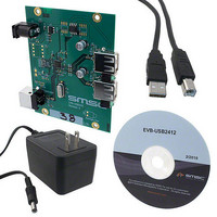
Manufacturer Part Number
EVB-USB2412
Description
EVALUATION BOARD FOR USB2412
Manufacturer
SMSC
Specifications of EVB-USB2412
Design Resources
EVB-USB2412 Schematic EVB-USB2412 BOM
Main Purpose
Interface, USB 2.0 Hub
Embedded
No
Utilized Ic / Part
USB2421
Primary Attributes
Dual Port Hub, High Speed (480Mbps)
Secondary Attributes
Single 5V Supply
Lead Free Status / RoHS Status
Lead free / RoHS Compliant
Other names
638-1106


Revision 0.2 (02-02-10)
2.1.5
Layout Considerations
The EVB-USB2412 is designed on four PCB layers--two signal layers and two ground layers. The PCB
layer stackup is shown in
with ground floods. Internal layers are ground. Note that the differential signals from the USB2412
match the upstream and downstream port placement simplifying the routing of the critical USB signals.
COMPONENT SIDE
Layer 2 -- GND
Layer 3 -- GND
Solder mask
Solder mask
Solder Side
Pre-preg
Pre-preg
Layer 1
Layer 4
Core
Table
Table 2.2 PCB Layer Stack
2.2. All signals and power are routed on top and bottom layers, along
USER MANUAL
4
4.25 mil, +/- 0.25 mil FR-4
4.25 mil, +/- 0.25 mil FR-4
1.8 - 3.1 mil, finished
1.8 - 3.1 mil, finished
1.3 mil (nominal)
1.3 mil (nominal)
EVB-USB2412 Evaluation Board User Manual
~24 mil FR-4
SMSC EVB-USB2412
Related parts for EVB-USB2412
Image
Part Number
Description
Manufacturer
Datasheet
Request
R

Part Number:
Description:
BOARD EVAL FOR USB2514 48-QFN
Manufacturer:
SMSC
Datasheet:

Part Number:
Description:
Networking Modules & Development Tools LAN7500 USB 2.0 BRD 10/100/1000 GigB
Manufacturer:
SMSC
Datasheet:

Part Number:
Description:
BOARD EVAL FOR USB2514/USB2514I
Manufacturer:
SMSC
Datasheet:

Part Number:
Description:
BOARD EVAL FOR USB2512/USB2512I
Manufacturer:
SMSC
Datasheet:

Part Number:
Description:
BOARD EVAL FOR USB2513/USB2513I
Manufacturer:
SMSC
Datasheet:

Part Number:
Description:
BOARD EVALUATION FOR EMC1043
Manufacturer:
SMSC
Datasheet:
Part Number:
Description:
EVALUATION BOARD FOR USB3311C
Manufacturer:
SMSC
Datasheet:
Part Number:
Description:
EVALUATION BOARD FOR USB3317C
Manufacturer:
SMSC
Datasheet:

Part Number:
Description:
EVALUATION BOARD USB2241-AEZG
Manufacturer:
SMSC
Datasheet:

Part Number:
Description:
BOARD EVAL USB2524 SHARE/SWITCH
Manufacturer:
SMSC
Datasheet:

Part Number:
Description:
BOARD EVALUATION FOR USB2502
Manufacturer:
SMSC
Datasheet:
Part Number:
Description:
BOARD EVALUATION FOR USB2504
Manufacturer:
SMSC
Datasheet:

Part Number:
Description:
EVALUATION BOARD LAN9500-ABZJ
Manufacturer:
SMSC
Datasheet:
Part Number:
Description:
Ethernet Modules & Development Tools LAN9500 Design Kit Low-Cost USB Dongle
Manufacturer:
SMSC
Datasheet: