EVAL-ADF4154EBZ1 Analog Devices Inc, EVAL-ADF4154EBZ1 Datasheet - Page 20
EVAL-ADF4154EBZ1
Manufacturer Part Number
EVAL-ADF4154EBZ1
Description
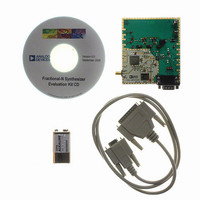
BOARD EVALUATION FOR ADF4154EB1
Manufacturer
Analog Devices Inc
Datasheet
1.ADF4154BRUZ.pdf
(24 pages)
Specifications of EVAL-ADF4154EBZ1
Main Purpose
Timing, Frequency Synthesizer
Embedded
No
Utilized Ic / Part
ADF4154
Primary Attributes
Single Fractional-N PLL
Secondary Attributes
19.2MHz PFD, Graphical User Interface
Lead Free Status / RoHS Status
Lead free / RoHS Compliant


ADF4154
In low spur mode (dither enabled), the repeat length is
extended to 2
makes the quantization error spectrum appear as broadband
noise. This can degrade the in-band phase noise at the PLL
output by as much as 10 dB. Therefore, for lowest noise, dither
off is a better choice, particularly when the final loop BW is low
enough to attenuate even the lowest frequency fractional spur.
Integer Boundary Spurs
Another mechanism for fractional spur creation are interactions
between the RF VCO frequency and the reference frequency.
When these frequencies are not integer related (as is the case
with fractional-N synthesizers), spur sidebands appear on the
VCO output spectrum at an offset frequency that corresponds
to the beat note or the difference in frequency between an
integer multiple of the reference and the VCO frequency.
These spurs are attenuated by the loop filter and are more
noticeable on channels close to integer multiples of the
reference, where the difference frequency can be inside the loop
bandwidth, thus the name integer boundary spurs.
Reference Spurs
Reference spurs are generally not a problem in fractional-N
synthesizers because the reference offset is far outside the loop
bandwidth. However, any reference feedthrough mechanism
that bypasses the loop can cause a problem. One such
mechanism is feedthrough of low levels of on-chip reference
switching noise through the RF
in reference spur levels as high as –90 dBc. Care should be
taken in the PCB layout to ensure that the VCO is well
separated from the input reference to avoid a possible feed-
through path on the board.
SPUR CONSISTENCY
When jumping from Frequency A to Frequency B and then
back again using fractional-N synthesizers, the spur levels often
differ each time Frequency A is programmed. However, in the
ADF4154, the spur levels on any particular channel are always
consistent.
FILTER DESIGN—ADIsimPLL
A filter design and analysis program is available to help the user
implement the PLL design. Visit
download of the ADIsimPLL software. The software designs,
simulates, and analyzes the entire PLL frequency and time
domain response. Various passive and active filter architectures
are allowed.
INTERFACING
The ADF4154 has a simple, SPI®-compatible serial interface for
writing to the device. SCLK, SDATA, and LE control the data
transfer. When LE (latch enable) is high, the 22 bits that have
been clocked into the input register on each rising edge of
SCLK are transferred to the appropriate latch. See Figure 2 for
the timing diagram and Table 5 for the latch truth table.
21
cycles, regardless of the value of MOD, which
IN
www.analog.com/pll
pin back to the VCO, resulting
for a free
Rev. A | Page 20 of 24
The maximum allowable serial clock rate is 20 MHz. This
means that the maximum update rate possible for the device is
909 kHz or one update every 1.1 μs.
ADuC812 Interface
Figure 21 shows the interface between the ADF4154 and the
ADuC812 MicroConverter®. Because the ADuC812 is based on
an 8051 core, this interface can be used with any 8051-based
microcontroller. The MicroConverter is set up for SPI master
mode with CPHA set to 0. To initiate the operation, bring the
I/O port driving LE low. Each latch of the ADF4154 requires a
24-bit word, which is accomplished by writing three 8-bit bytes
from the MicroConverter to the device. After the third byte is
written, the LE input should be brought high to complete the
transfer.
When operating in the mode described, the maximum
SCLOCK rate of the ADuC812 is 4 MHz. This means that the
maximum rate at which the output frequency can be changed is
180 kHz.
ADSP-21xx Interface
Figure 22 shows the interface between the ADF4154 and the
ADSP-21xx digital signal processor. As discussed previously, the
ADF4154 requires a 24-bit serial word for each latch write. The
easiest way to accomplish this using a device in the ADSP-21xx
family is to use the autobuffered transmit mode of operation
with alternate framing. This provides a means for transmitting
an entire block of serial data before an interrupt is generated.
Set up the word length for eight bits and use three memory
locations for each 24-bit word. To program each 24-bit latch,
store each of the three 8-bit bytes, enable the autobuffered
mode, and write to the transmit register of the DSP. This last
operation initiates the autobuffered transfer.
ADSP-21xx
ADuC812
I/O PORTS
I/O FLAGS
SCLOCK
SCLOCK
Figure 22. ADSP-21xx-to-ADF4154 Interface
Figure 21. ADuC812-to-ADF4154 Interface
MOSI
TFS
DT
SCLK
SDATA
LE
MUXOUT
(LOCK DETECT)
SCLK
SDATA
LE
MUXOUT
(LOCK DETECT)
ADF4154
ADF4154
Related parts for EVAL-ADF4154EBZ1
Image
Part Number
Description
Manufacturer
Datasheet
Request
R

Part Number:
Description:
IC, ADJ LDO REG, 1.5V TO 5V 250mA MSOP-8
Manufacturer:
Vishay
Datasheet:

Part Number:
Description:
IC, ADJ LDO REG, 1.5V TO 5V 0.6A 8-TSSOP
Manufacturer:
Vishay
Datasheet:
Part Number:
Description:
IC, ADJ LDO REG, 1.5V TO 5V 250mA MSOP-8
Manufacturer:
Vishay
Datasheet:

Part Number:
Description:
IC ADJ LDO REG 1.5V TO 5V 150mA 5-SOT-23
Manufacturer:
Vishay
Datasheet:

Part Number:
Description:
BOARD EVAL AS1324-AD
Manufacturer:
austriamicrosystems
Datasheet:
Part Number:
Description:
IC, ADJ LDO REG, 1.5V TO 5V 0.6A 8-TSSOP
Manufacturer:
Vishay
Datasheet:

Part Number:
Description:
IC, ADJ LDO REG, 1.5V TO 5V, 0.3A, MSOP8
Manufacturer:
Vishay
Datasheet:
Part Number:
Description:
IC, ADJ LDO REG, 1.5V TO 5V, 0.3A, MSOP8
Manufacturer:
Vishay
Datasheet:
Part Number:
Description:
IC, ADJ LDO REG 1.215V TO 5V 0.3A MSOP-8
Manufacturer:
Vishay
Datasheet:
Part Number:
Description:
IC, ADJ LDO REG 1.215V TO 5V 0.3A MSOP-8
Manufacturer:
Vishay
Datasheet:

Part Number:
Description:
±1.7g Dual-Axis IMEMS Accelerometer Evaluation Board
Manufacturer:
Analog Devices Inc
Datasheet:

Part Number:
Description:
IC MULTIPLIER ANALOG 8-SOIC T/R
Manufacturer:
Analog Devices Inc
Datasheet:

Part Number:
Description:
IC ANALOG MULTIPLIER 8-DIP
Manufacturer:
Analog Devices Inc
Datasheet:
Part Number:
Description:
IC ANALOG MULTIPLIER 8-SOIC
Manufacturer:
Analog Devices Inc
Datasheet:
Part Number:
Description:
IC ANALOG MULTIPLIER 8-DIP
Manufacturer:
Analog Devices Inc
Datasheet: