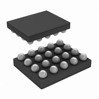
LP8720TLX-B/NOPB National Semiconductor, LP8720TLX-B/NOPB Datasheet - Page 3

LP8720TLX-B/NOPB
Manufacturer Part Number
LP8720TLX-B/NOPB
Description
IC REG BUCK 5-LDO I2C 20USMD
Manufacturer
National Semiconductor
Datasheet
1.LP8720TLENOPB.pdf
(24 pages)
Specifications of LP8720TLX-B/NOPB
Topology
Step-Down (Buck) Synchronous (1), Linear (LDO) (5)
Function
Any Function
Number Of Outputs
6
Frequency - Switching
2MHz
Voltage/current - Output 1
0.8 V ~ 2.3 V, 400mA
Voltage/current - Output 2
1.2 V ~ 3.3 V, 300mA
Voltage/current - Output 3
1.2 V ~ 3.3 V, 300mA
W/led Driver
No
W/supervisor
No
W/sequencer
Yes
Voltage - Supply
2.7 V ~ 4.5 V
Operating Temperature
-40°C ~ 85°C
Mounting Type
Surface Mount
Package / Case
20-UFBGA
Lead Free Status / RoHS Status
Lead free / RoHS Compliant
Available stocks
Company
Part Number
Manufacturer
Quantity
Price
Part Number:
LP8720TLX-B/NOPB
Manufacturer:
TI/德州仪器
Quantity:
20 000
LP8720 Pin Descriptions
Pin Number
D1
C1
D2
D4
C4
C3
C2
D3
A4
E4
A2
B4
A3
A1
E1
E3
B1
B3
E2
B2
A:
D
I
DI/O
G
O
P
DEFSEL
VBATT
IRQ_N
GNDB
IDSEL
Name
LDO1
LDO2
LDO3
LDO4
LDO5
VINB
VIN1
VIN2
GND
SDA
SCL
DVS
SW
EN
FB
Analog Pin
Digital Pin
Input Pin
Digital Input/Output Pin
Ground
Output Pin
Power Connection
Type
DI/O
DO
DI
DI
DI
DI
DI
G
G
P
P
P
P
A
A
A
A
A
A
A
Description
Battery Input for LDO1 and all internal circuitry.
Battery Input for Buck.
Battery Input for LDO2 and LDO3.
Battery Input for LDO4 and LDO5.
LDO1 Output.
LDO2 Output.
LDO3 Output.
LDO4 Output.
LDO5 Output.
Buck Output.
Buck Feedback.
Power Ground for Buck.
IC Ground.
I
is needed, typ 1.5 kΩ. If not in use then hard wire to GND.
I
not in use then hard wire to GND.
Interrupt output, active LOW. Open Drain output, external pull up resistor is needed, typ
10 kΩ. If not in use then hard wire to GND or leave floating.
Enable. EN=LO standby. EN=HI power on. Internal pull down resistor 500 kΩ.
If not in use then hard wire to VBATT.
Control input that sets the default voltages and startup sequence. Must be hard wired to BATT
or GND or left floating (Hi-Z) for specific application.
When DEFSEL= VBATT then setup 1 is used for default voltages and startup sequence.
When DEFSEL= GND then setup 2 is used for default voltages and startup sequence.
When DEFSEL= floating (Hi-Z) setup 3 is used for default voltages and startup sequence.
Control input that sets the slave address for serial interface. Must be hard wired to BATT or
GND or left floating (Hi-Z) for specific application.
When IDSEL= VBATT then slave address is 7h’7F
When IDSEL= floating (Hi-Z) then slave address is 7h’7C
When IDSEL= GND then slave address is 7h’7D
Dynamical Voltage Scaling.
When DVS=HI then Buck voltage set BUCK_V1 is in use.
When DVS=LO then Buck voltage set BUCK_V2 is in use.
Buck voltage set BUCK_V1 should be higher than Buck voltage set BUCK_V2.
If not in use then hard wire to VBATT or GND.
2
2
C-compatible Serial Interface Data Input/Output. Open Drain output, external pull up resistor
C-compatible Serial Interface Clock input. External pull up resistor is needed, typ 1.5 kΩ. If
3
www.national.com


