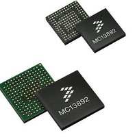
MC13892JVL Freescale Semiconductor, MC13892JVL Datasheet - Page 14

MC13892JVL
Manufacturer Part Number
MC13892JVL
Description
IC PMU I.MX51/37/35/27 186MAPBGA
Manufacturer
Freescale Semiconductor
Datasheets
1.MC13892AJVLR2.pdf
(156 pages)
2.MC13892AJVLR2.pdf
(2 pages)
3.MC13892AJVLR2.pdf
(16 pages)
4.MC13892JVL.pdf
(161 pages)
Specifications of MC13892JVL
Applications
Battery Management, Display (LED Drivers), Handheld/Mobile Devices, Power Supply
Operating Temperature
-40°C ~ 85°C
Mounting Type
Surface Mount
Package / Case
186-LFBGA
Output Current
65 mA
Output Voltage
1.5 V
Operating Temperature (max)
85C
Operating Temperature (min)
-40C
Mounting
Surface Mount
Package Type
BGA
Case Length
12mm
Screening Level
Industrial
Lead Free Status / RoHS Status
Lead free / RoHS Compliant
Current - Supply
-
Voltage - Supply
-
Lead Free Status / Rohs Status
Lead free / RoHS Compliant
Available stocks
Company
Part Number
Manufacturer
Quantity
Price
Company:
Part Number:
MC13892JVL
Manufacturer:
DALSA
Quantity:
4
Company:
Part Number:
MC13892JVL
Manufacturer:
Freescale Semiconductor
Quantity:
10 000
Part Number:
MC13892JVL
Manufacturer:
FREESCALE
Quantity:
20 000
Company:
Part Number:
MC13892JVLR2
Manufacturer:
Freescale Semiconductor
Quantity:
10 000
ELECTRICAL CHARACTERISTICS
STATIC ELECTRICAL CHARACTERISTICS
Table 5. Static Electrical Characteristics
the approximate parameter means at T
14
13892
BUCK CONVERTERS (CONTINUED)
SWBST
Notes
Effective Quiescent Current Consumption
Automatic Mode Change Threshold, Switchover between PFM and PWM
modes
Efficiency
External Components, Used as a condition for all other parameters
Average Output Voltage
Output Ripple
Average Load Regulation
Average Line Regulation
16.
17.
18.
19.
20.
21.
Characteristics noted under conditions - 30°C ≤ T
PWM Mode, IL = 0 mA; device not switching
PFM Mode, IL = 0 mA; device not switching
PFM, 0.9 V, 1.0 mA
PFM, 01.8 V, 1.0 mA
PWM Pulse Skipping, 1.25 V, 50 mA
PWM Pulse Skipping, 1.8 V, 50 mA
PWM, 1.25 V, 500 mA
PWM, 1.8 V, 500 mA
Inductor for SW2, SW3, SW4
Inductor for SW1
Inductor Resistance
Bypass Capacitor for SW2, SW3, SW4
Bypass Capacitor for SW1
Bypass Capacitor ESR
Input Capacitor
3.0 V < V
3.0 V < V
Schottky diode
V
3.0 V < V
IN
Preferred device TDK VLS252012 series at 2.5x2.0 mm footprint and 1.2 mm max height
Preferably 0603 style 6.3 V rated X5R/X7R type at 35% total make tolerance, temperature spread and DC bias derating such as TDK
C1608X5R0J106M
Preferably 0805 style 6.3 V rated X5R/X7R type at 35% total make tolerance, temperature spread and DC bias derating such as TDK
C2012X5R0J226M
Preferably 0603 style 6.3 V rated X5R/X7R type at 35% total make tolerance, temperature spread and DC bias derating such as TDK
C1608X5R0J475
Output voltage when configured to supply VBUS in OTG mode can be as high as 5.75 V
Vin is the low side of the inductor that is connected to BP.
= 3.6 V, 0 < IL < IL
IN
IN
IN
< 4.65, 0 < IL < IL
< 4.65 V, IL = IL
< 4.65 (1), 0 < IL < IL
(19)
(16)
(20)
MAX
Characteristic
(18)
MAX
(16)
MAX
MAX
, Excluding reverse recovery of
(21)
(17)
A =
25 °C under nominal conditions, unless otherwise noted.
A
≤ 85 °C, GND = 0 V unless otherwise noted. Typical values noted reflect
VBSTLOR
VBSTLIR
C
Symbol
AMC
ESR
V
L
C
I
R
OSW234
VBST
L
SWQS
SW234
BSTPP
OSW1
WSW
SW1
SW
TH
Nom-5%
-20%
-30%
-35%
-35%
Min
5.0
1.0
-
-
-
-
-
-
-
-
-
-
-
-
-
Analog Integrated Circuit Device Data
2x22
Typ
2.2
1.5
4.7
5.0
50
15
50
75
85
78
82
78
82
10
-
-
-
-
-
Freescale Semiconductor
Nom+5%
+20%
+30%
+35%
+35%
Max
0.16
100
120
0.5
30
50
50
-
-
-
-
-
-
-
-
mV/mA
mVpp
Unit
mΩ
mA
mV
µH
µH
µA
µF
µF
µF
W
%
V


