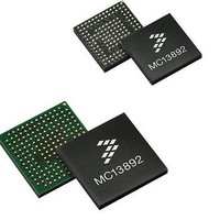
MC13892BJVL Freescale Semiconductor, MC13892BJVL Datasheet - Page 14

MC13892BJVL
Manufacturer Part Number
MC13892BJVL
Description
IC PMU I.MX51/37/35/27 186MAPBGA
Manufacturer
Freescale Semiconductor
Datasheets
1.MC13892AJVLR2.pdf
(156 pages)
2.MC13892AJVLR2.pdf
(2 pages)
3.MC13892AJVLR2.pdf
(16 pages)
4.MC13892AJVLR2.pdf
(5 pages)
Specifications of MC13892BJVL
Applications
Battery Management, Display (LED Drivers), Handheld/Mobile Devices, Power Supply
Operating Temperature
-40°C ~ 85°C
Mounting Type
Surface Mount
Package / Case
186-LFBGA
Mounting Style
SMD/SMT
Duty Cycle (max)
55 %
Input Voltage
- 0.3 V to + 20 V
Maximum Operating Temperature
+ 85 C
Minimum Operating Temperature
- 30 C
Output Current
30 mA
Output Voltage
3.3 V
Topology
Boost
Lead Free Status / RoHS Status
Lead free / RoHS Compliant
Current - Supply
-
Voltage - Supply
-
Lead Free Status / Rohs Status
Lead free / RoHS Compliant
Available stocks
Company
Part Number
Manufacturer
Quantity
Price
Company:
Part Number:
MC13892BJVL
Manufacturer:
Freescale Semiconductor
Quantity:
10 000
Company:
Part Number:
MC13892BJVLR2
Manufacturer:
Freescale Semiconductor
Quantity:
10 000
LDO AND BATTERY CHARGER ROUTING
Figure 17. Recommended Configuration.
8
LDO and Battery Charger Routing
The LDOs and battery charger do not handle much current in this application, so their routing is not critical. The
same philosophy must be followed for current handling on the traces though.
For a proper functionality of these supplies, bypass and output capacitors must be placed near the IC to achieve a
good width and shortness of the traces. The ESR of the output capacitors of the external PNP LDOs must be
between 20 and 100 mΩ, in order to achieve good stability. If they are not within these values, an additional resistor
will be needed. This resistance can be achieved with a copper trace on the board and is also a cost saving.
The critical signals for the charger that must not be contaminated by high frequency or power ones are highlighted
in
Figure
18.
Figure 18. Critical Signals on the Battery Charger.
The sense lines should be routed from the sense resistor endpoints and should not be included in high current
charge path. They should also have a maximum of 1.0 nH parasitic inductance and 30 mΩ of resistance.
Charge path can handle up to 1600 mA, so following the rule listed previously, for 1.0 oz copper, the trace width must
be at least 16 mils.
As a placement suggestion, the thermistor must be located as close to the battery as possible for a correct
temperature reading.
13892
Analog Integrated Circuit Device Data
14
Freescale Semiconductor


