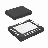
LP3906SQ-TKXII/NOPB National Semiconductor, LP3906SQ-TKXII/NOPB Datasheet - Page 24

LP3906SQ-TKXII/NOPB
Manufacturer Part Number
LP3906SQ-TKXII/NOPB
Description
IC REG BUCK/LDO DUAL 1.5A 300MA
Manufacturer
National Semiconductor
Series
PowerWise®r
Datasheet
1.LP3906SQ-DJXINOPB.pdf
(40 pages)
Specifications of LP3906SQ-TKXII/NOPB
Applications
Digital Cores
Current - Supply
60µA
Voltage - Supply
2.7 V ~ 5.5 V
Operating Temperature
-40°C ~ 85°C
Mounting Type
Surface Mount
Package / Case
24-WFQFN Exposed Pad
Lead Free Status / RoHS Status
Lead free / RoHS Compliant
www.national.com
INTERRUPT STATUS REGISTER (ISRA) 0X02
This register informs the user of the temperature status of the chip.
CONTROL 1 REGISTER (SCR1) 0X07
This register allows the user to select the preset delay sequence for power-on timing, to switch between PFM and PWM mode for
the bucks, and also to select between an internal and external clock for the bucks.
The external LDO and SW enables should be pulled LOW to allow the blocks to sequence correctly through assertion of the EN_T
pin.
EN_DLY PRESET DELAY SEQUENCE AFTER EN_T ASSERTION
Name
Access
Data
Reset
Name
Access —
Data
Reset
EN_DLY<2:0>
D7
—
Reserved
0
D7-2
—
—
Reserved
0
000
001
010
011
100
101
110
111
D6-4
EN_DLY
R/W
Selects the preset
delay sequence
from EN_T assertion
(shown below)
010
D1
Temp 125°C
R
Status bit for thermal warning PMIC T>125°C
0
0 – PMIC Temp. < 125°C
1 – PMIC Temp. > 125°C
D3
—
—
Reserved
1
Buck1
1.5
1.5
1.5
1.5
1
1
3
2
D2
FPWM2
R/W
Buck 2 PWM /PFM
Mode select
0 – Auto Switch PFM -
PWM operation
1 – PWM Mode Only
0
24
Buck2
1.5
1.5
1
2
2
2
2
3
Delay (ms)
D1
FPWM1
R/W
Buck 1 PWM /PFM
Mode select
0 – Auto Switch PFM -
PWM operation
1 – PWM Mode Only
0
LDO1
1
2
3
1
3
2
1
6
D0
ECEN
R/W
External Buck Clock
Select
0 – Internal 2 MHz
Oscillator clock
1 – External 13 MHz
Oscillator clock
0
D0
—
—
Reserved
0
LDO2
1.5
11
1
2
6
1
6
2


