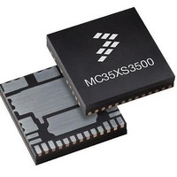
MC35XS3500PNA Freescale Semiconductor, MC35XS3500PNA Datasheet - Page 5

MC35XS3500PNA
Manufacturer Part Number
MC35XS3500PNA
Description
IC SWITCH HIGHSIDE 24PQFN
Manufacturer
Freescale Semiconductor
Type
High Side Switchr
Datasheet
1.MC35XS3500PNAR2.pdf
(41 pages)
Specifications of MC35XS3500PNA
Number Of Outputs
5
Rds (on)
*
Internal Switch(s)
Yes
Current Limit
9A
Voltage - Input
7 V ~ 20 V
Operating Temperature
-40°C ~ 125°C
Mounting Type
Surface Mount
Package / Case
24-PQFN, 24-PowerQFN
Product
MOSFET Gate Drivers
Rise Time
50 ns
Fall Time
50 ns
Propagation Delay Time
6.5 ms
Supply Voltage (max)
+ 5.5 V
Supply Voltage (min)
- 0.3 V
Supply Current
20 mA
Maximum Operating Temperature
+ 125
Minimum Operating Temperature
- 40 C
Lead Free Status / RoHS Status
Lead free / RoHS Compliant
Available stocks
Company
Part Number
Manufacturer
Quantity
Price
Analog Integrated Circuit Device Data
Freescale Semiconductor
Table 2. Maximum Ratings
permanent damage to the device.
ELECTRICAL RATINGS
THERMAL RATINGS
THERMAL RESISTANCE
Notes
Over-voltage Test Range
Reverse Polarity Voltage Range
VCC Supply Voltage
Output Voltage
Digital Input Current in Clamping Mode (SI, SCLK,
STOP, LIMP)
FETIN Input Current
SO and FETOUT Output Voltage
Outputs clamp energy using single pulse method (L = 2mH; R = 0 Ω;
VBAT = 14 V @ 150 °C initial)
ESD Voltage
Operating Temperature
Peak Pin Reflow Temperature During Solder Mounting
Storage Temperature
Thermal Resistance, Junction to Case
2.
3.
4.
All voltages are with respect to ground unless otherwise noted. Exceeding these ratings may cause a malfunction or
Maximum Operationg Voltage
Load Dump (400ms) @ 25 °C
2.0 Min @ 25 °C
Positive
Negative (ground disconnected)
Human Body Model (HBM) OUT[1:5], VPWR, and GND
Charge Device Model (CDM)
Ambient
Junction
ESD testing is performed in accordance with the Human Body Model (HBM) (C
Model.
Pin soldering temperature limit is for 40 seconds maximum duration. Not designed for immersion soldering. Exceeding these limits may
cause malfunction or permanent damage to the device. If the qualification fails, TSOLDER will be changed for 240
Typical value is guaranteed per design.
Corner Pins (1,13,19,21)
All Other Pins (2-12, 14-18, 20, 22-24)
(2)
Rating
(4)
ELECTRICAL CHARACTERISTICS
CS
, IGN, FLASHER,
(3)
MAXIMUM RATINGS
T
Symbol
I
SOLDER
V
V
V
V
T
FETIN
R
V
V
OUT
I
T
BAT
BAT
ESD
T
STG
E
θ
CC
IN
SO
A
J
JC
ZAP
= 100 pF, R
ZAP
- 0.3 to V
ELECTRICAL CHARACTERISTICS
-0.3 to 5.5
- 40 to 125
- 40 to 150
- 55 to 150
= 1500 Ω) and the Charge Device
± 2000
± 8000
Value
± 750
± 500
±1.0
+10
-1.0
260
- 18
-16
1.0
28
40
40
30
CC
+ 0.3
MAXIMUM RATINGS
°C.
35XS3500
°
Unit
mA
mA
K/W
mJ
°Χ
°Χ
°C
V
V
V
V
V
V
5


