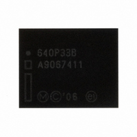
PC28F640P33B85A NUMONYX, PC28F640P33B85A Datasheet - Page 8

PC28F640P33B85A
Manufacturer Part Number
PC28F640P33B85A
Description
IC FLASH 64MBIT 85NS 64EZBGA
Manufacturer
NUMONYX
Series
StrataFlash™r
Datasheet
1.PC28F640P33B85A.pdf
(96 pages)
Specifications of PC28F640P33B85A
Format - Memory
FLASH
Memory Type
FLASH
Memory Size
64M (4M x 16)
Speed
85ns
Interface
Parallel
Voltage - Supply
2.3 V ~ 3.6 V
Operating Temperature
-40°C ~ 85°C
Package / Case
64-TBGA
Cell Type
NOR
Density
64Mb
Access Time (max)
85ns
Interface Type
Parallel/Serial
Boot Type
Bottom
Address Bus
22b
Operating Supply Voltage (typ)
2.5/3/3.3V
Operating Temp Range
-40C to 85C
Package Type
EZBGA
Sync/async
Async/Sync
Operating Temperature Classification
Industrial
Operating Supply Voltage (min)
2.3V
Operating Supply Voltage (max)
3.6V
Word Size
16b
Number Of Words
4M
Supply Current
28mA
Mounting
Surface Mount
Pin Count
64
Lead Free Status / RoHS Status
Lead free / RoHS Compliant
Other names
888226
888226
PC28F640P33B85
PC28F640P33B85 888226
888226
PC28F640P33B85
PC28F640P33B85 888226
Available stocks
Company
Part Number
Manufacturer
Quantity
Price
Company:
Part Number:
PC28F640P33B85A
Manufacturer:
Micron Technology Inc
Quantity:
10 000
2.0
2.1
Datasheet
8
Functional Overview
This section provides an overview of the features and capabilities of the Numonyx™
StrataFlash
The Kearny Family Flash memory provides density upgrades from 64-Mbit through 512-
Mbit. This family of devices provides high performance at low voltage on a 16-bit data
bus. Individually erasable memory blocks are sized for optimum code and data storage.
Upon initial power up or return from reset, the device defaults to asynchronous page-
mode read. Configuring the RCR enables synchronous burst-mode reads. In
synchronous burst mode, output data is synchronized with a user-supplied clock signal.
A WAIT signal provides an easy CPU-to-flash memory synchronization.
In addition to the enhanced architecture and interface, the device incorporates
technology that enables fast factory program and erase operations. Designed for low-
voltage systems, the Kearny Family Flash memory supports read operations with V
3.0V, and erase and program operations with V
fastest flash array programming performance with V
throughput. With V
power design. In addition to voltage flexibility, a dedicated VPP connection provides
complete data protection when V
The CUI is the interface between the system processor and all internal operations of
the device. An internal WSM automatically executes the algorithms and timings
necessary for block erase and program. A Status Register indicates erase or program
completion and any errors that may have occurred.
An industry-standard command sequence invokes program and erase automation. Each
erase operation erases one block. The Erase Suspend feature allows system software to
pause an erase cycle to read or program data in another block. Program Suspend
allows system software to pause programming to read other locations. Data is
programmed in word increments (16 bits).
The Kearny Family Flash memory protection register allows unique flash device
identification that can be used to increase system security. The individual Block Lock
feature provides zero-latency block locking and unlocking. In addition, the Kearny
Family Flash memory may also pre-define main array space as OTP.
Virtual Chip Enable Description
The 512 Mbit Kearny Family Flash memory employs a Virtual Chip Enable which
combines two 256-Mbit die with a common chip enable, F1-CE# for QUAD+ packages
or CE# for Easy BGA packages (refer to
Address A24 (QUAD+ package) or A25 (Easy BGA and TSOP package) is then used to
select between the die pair with F1-CE# / CE# asserted, depending upon the package
option used. When chip enable is asserted and QUAD+ A24 (Easy BGA A25) is low
(
A24 (Easy BGA A25) is high (
“Flash Die Virtual Chip Enable Truth Table for 512 Mbit QUAD+ Package”
“Flash Die Virtual Chip Enable Truth Table for 512 Mbit TSOP / Easy BGA Package”
additional details.
V
IL
), The lower parameter die is selected; when chip enable is asserted and QUAD+
®
Embedded Memory (P33) device.
PP
at 3.0V, VCC and VPP can be tied together for a simple, ultra low
V
IH
), the upper parameter die is selected. Refer to
PP
≤ V
PPLK
Figure 10
.
Numonyx™ StrataFlash
PP
at 3.0V or 9.0V. BEFP provides the
and
PP
Figure 11
at 9.0V, which increases factory
®
for additional details).
Embedded Memory (P33)
Order Number: 314749-05
and
November 2007
Table 2,
Table 1,
CC
for
at


