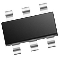
MCP65R41T-2402E/CHY Microchip Technology, MCP65R41T-2402E/CHY Datasheet - Page 23

MCP65R41T-2402E/CHY
Manufacturer Part Number
MCP65R41T-2402E/CHY
Description
IC COMPARATOR 2.4V REF SOT-23-6
Manufacturer
Microchip Technology
Type
General Purposer
Datasheet
1.MCP65R41T-1202ECHY.pdf
(34 pages)
Specifications of MCP65R41T-2402E/CHY
Output Type
CMOS, Push-Pull, TTL
Package / Case
*
Number Of Elements
1
Voltage - Supply
1.8 V ~ 5.5 V
Mounting Type
Surface Mount
Product
Digital Comparators
Offset Voltage (max)
10 mV
Input Bias Current (max)
1 pA
Supply Voltage (max)
5.5 V
Supply Voltage (min)
1.8 V
Maximum Operating Temperature
+ 125 C
Mounting Style
SMD/SMT
High Level Output Current
- 100 nA
Minimum Operating Temperature
- 40 C
Comparator Type
Low Power
No. Of Comparators
1
Ic Output Type
Push Pull
Output Compatibility
CMOS, TTL
Supply Current
2.5µA
Supply Voltage Range
1.8V To 5.5V
Amplifier Case Style
SOT-23
Rohs Compliant
No
Lead Free Status / RoHS Status
Lead free / RoHS Compliant
Other names
MCP65R41T-2402E/CHY
MCP65R41T-2402E/CHYTR
MCP65R41T-2402E/CHYTR
Available stocks
Company
Part Number
Manufacturer
Quantity
Price
Company:
Part Number:
MCP65R41T-2402E/CHY
Manufacturer:
RENESAS
Quantity:
694
Company:
Part Number:
MCP65R41T-2402E/CHY
Manufacturer:
Microchip Technology
Quantity:
135
4.3.2
Figure 4-6
using three resistors. The resulting hysteresis diagram
is shown in
FIGURE 4-6:
Hysteresis.
FIGURE 4-7:
Inverting Circuit.
In order to determine the trip voltages (V
for the circuit shown in
simplified to the Thevenin equivalent circuit with
respect to V
FIGURE 4-8:
2010 Microchip Technology Inc.
* Pull-up resistor required for the MCP65R46 only.
V
V
V
V
* Pull-up resistor required for the MCP65R46 only.
OH
DD
OL
SS
V
V
23
Where:
V
SS
IN
R
R
Low-to-High
V
2
3
shows an inverting circuit for single-supply
V
OUT
INVERTING CIRCUIT
Figure
REF
REF
R
, as shown in
23
4-7.
V
R
23
V
23
TLH
Inverting Circuit with
Hysteresis Diagram for the
Thevenin Equivalent Circuit.
=
=
Figure
V
+
-
DD
------------------ -
R
------------------ -
R
V
2
R
2
THL
V
R
+
2
Figure
+
3
DD
R
R
R
4-6, R
R
3
F
High-to-Low
3
V
3
R
SS
V
V
F
PU
4-8:
REF
2
V
R
and R
PU
PU
THL
V
V
R
*
DD
OUT
PU
and V
3
V
*
can be
OUT
V
IN
TLH
)
By using this simplified circuit, the trip voltage can be
calculated using the following equation:
EQUATION 4-1:
Figures 2-23
typical values for V
4.4
With this family of comparators, the power supply pin
(V
capacitor (i.e., 0.01 µF to 0.1 µF) within 2 mm for good
edge rate performance.
4.5
4.5.1
Reasonable capacitive loads (e.g., logic gates) have
little impact on the propagation delay (see
The supply current increases with the increasing toggle
frequency
capacitive loads. The output slew rate and propagation
delay performance will be reduced with higher capaci-
tive loads.
4.5.2
The reference output is designed to interface to the
comparator input pins, either directly or with some
resistive network, such as voltage divider network, with
minimal capacitive load. The recommended capacitive
load is 200 pF (typical). Capacitive loads greater than
2000 pF may cause the V
power up.
DD
for single supply) should have a local bypass
Where:
V
V
V
V
TLH
THL
THL
TLH
Bypass Capacitors
Capacitive Loads
OUT PIN
V
= trip voltage from low to high
= trip voltage from high to low
(Figure
=
=
and
REF
V
V
OH
OL
PIN
2-26
OH
2-22),
MCP65R41/6
---------------------- -
R
---------------------- -
R
and V
23
23
R
R
can be used to determine the
+
+
23
23
R F
R F
REF
OL
especially
.
+
+
output to oscillate at
V
V
23
23
DS22269A-page 23
--------------------- -
R
--------------------- -
R
23
23
R
R
Figure
with
+
+
F
F
R
R
F
F
higher
2-34).


