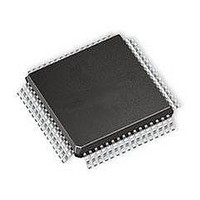
PIC16LF1527-I/PT Microchip Technology, PIC16LF1527-I/PT Datasheet - Page 137

PIC16LF1527-I/PT
Manufacturer Part Number
PIC16LF1527-I/PT
Description
MCU PIC 28KB FLASH 64TQFP
Manufacturer
Microchip Technology
Series
PIC® XLP™ 16Fr
Datasheet
1.PIC16LF1526T-IPT.pdf
(354 pages)
Specifications of PIC16LF1527-I/PT
Core Processor
PIC
Core Size
8-Bit
Speed
20MHz
Connectivity
I²C, LIN, SPI, UART/USART
Peripherals
Brown-out Detect/Reset, POR, PWM, WDT
Number Of I /o
54
Program Memory Size
28KB (16K x 14)
Program Memory Type
FLASH
Ram Size
1.5K x 8
Voltage - Supply (vcc/vdd)
1.8 V ~ 3.6 V
Data Converters
A/D 30x10b
Oscillator Type
Internal
Operating Temperature
-40°C ~ 85°C
Package / Case
64-TQFP
Processor Series
PIC16F
Core
PIC
Data Ram Size
768 B
Interface Type
MI2C, SPI, EUSART
Number Of Timers
9
Operating Supply Voltage
1.8 V to 5.5 V
Maximum Operating Temperature
+ 85 C
Mounting Style
SMD/SMT
Development Tools By Supplier
MPLAB IDE Software
Minimum Operating Temperature
- 40 C
Lead Free Status / RoHS Status
Lead free / RoHS Compliant
Eeprom Size
-
Lead Free Status / Rohs Status
Details
Available stocks
Company
Part Number
Manufacturer
Quantity
Price
Company:
Part Number:
PIC16LF1527-I/PT
Manufacturer:
MICROCHIP
Quantity:
2 100
Company:
Part Number:
PIC16LF1527-I/PT
Manufacturer:
Microchip Technology
Quantity:
10 000
- Current page: 137 of 354
- Download datasheet (3Mb)
12.8
PORTG is a 6-bit wide, bidirectional port. The
corresponding data direction register is TRISG
(Register
corresponding PORTG pin an input (i.e., disable the
output driver). Clearing a TRISG bit (= 0 ) will make the
corresponding PORTG pin an output (i.e., enables
output driver and puts the contents of the output latch
on the selected pin). The exception is RG5, which is
input only and its TRIS bit will always read as ‘ 1 ’.
Example 12-1
Reading the PORTG register
status of the pins, whereas writing to it will write to the
PORT latch. All write operations are read-modify-write
operations. Therefore, a write to a port implies that the
port pins are read, this value is modified and then
written to the PORT data latch (LATG).
The TRISG register
PORTG pin output drivers, even when they are being
used as analog inputs. The user should ensure the bits
in the TRISG register are maintained set when using
them as analog inputs. I/O pins configured as analog
input always read ‘ 0 ’.
12.8.1
The ANSELG register
configure the Input mode of an I/O pin to analog.
Setting the appropriate ANSELG bit high will cause all
digital reads on the pin to be read as ‘ 0 ’ and allow
analog functions on the pin to operate correctly.
The state of the ANSELG bits has no effect on digital
output functions. A pin with TRIS clear and ANSEL set
will still operate as a digital output, but the Input mode
will be analog. This can cause unexpected behavior
when executing read-modify-write instructions on the
affected port.
2011 Microchip Technology Inc.
Note:
PORTG Registers
12-3). Setting a TRISG bit (= 1 ) will make the
ANSELG REGISTER
The ANSELG bits default to the Analog
mode after Reset. To use any pins as
digital general purpose or peripheral
inputs, the corresponding ANSEL bits
must be initialized to ‘ 0 ’ by user software.
shows how to initialize an I/O port.
(Register
(Register
(Register
12-3) controls the
12-5) is used to
12-2) reads the
Preliminary
12.8.2
Each PORTG pin is multiplexed with other functions. The
pins, their combined functions and their output priorities
are shown in
When multiple outputs are enabled, the actual pin
control goes to the peripheral with the highest priority.
Analog input functions, such as ADC, are not shown in
the priority lists. These inputs are active when the I/O
pin is set for Analog mode using the ANSELx registers.
Digital output functions may control the pin when it is in
Analog mode with
TABLE 12-16: PORTG OUTPUT PRIORITY
Note 1:
Pin Name
PIC16(L)F1526/27
RG0
RG1
RG2
RG3
RG4
RG5
Priority listed from highest to lowest.
PORTG FUNCTIONS AND OUTPUT
PRIORITIES
Table
Table
12-16.
12-16.
Function Priority
CCP3
RG0
CK2
TX2
RG1
DT2
RG2
CCP4
RG3
CCP5
RG4
Input only pin
DS41458A-page 137
(1)
Related parts for PIC16LF1527-I/PT
Image
Part Number
Description
Manufacturer
Datasheet
Request
R

Part Number:
Description:
IC, 8BIT MCU, PIC16LF, 32MHZ, QFN-28
Manufacturer:
Microchip Technology
Datasheet:

Part Number:
Description:
IC, 8BIT MCU, PIC16LF, 32MHZ, QFN-28
Manufacturer:
Microchip Technology
Datasheet:

Part Number:
Description:
IC, 8BIT MCU, PIC16LF, 32MHZ, DIP-18
Manufacturer:
Microchip Technology
Datasheet:

Part Number:
Description:
IC, 8BIT MCU, PIC16LF, 20MHZ, TQFP-44
Manufacturer:
Microchip Technology
Datasheet:

Part Number:
Description:
7 KB Flash, 384 Bytes RAM, 32 MHz Int. Osc, 16 I/0, Enhanced Mid Range Core, Nan
Manufacturer:
Microchip Technology

Part Number:
Description:
14KB Flash, 512B RAM, LCD, 11x10b ADC, EUSART, NanoWatt XLP 28 SOIC .300in T/R
Manufacturer:
Microchip Technology
Datasheet:

Part Number:
Description:
14KB Flash, 512B RAM, LCD, 11x10b ADC, EUSART, NanoWatt XLP 28 SSOP .209in T/R
Manufacturer:
Microchip Technology
Datasheet:

Part Number:
Description:
MCU PIC 14KB FLASH XLP 28-SSOP
Manufacturer:
Microchip Technology

Part Number:
Description:
MCU PIC 14KB FLASH XLP 28-SOIC
Manufacturer:
Microchip Technology

Part Number:
Description:
MCU PIC 512B FLASH XLP 28-UQFN
Manufacturer:
Microchip Technology

Part Number:
Description:
MCU PIC 14KB FLASH XLP 28-SPDIP
Manufacturer:
Microchip Technology

Part Number:
Description:
MCU 7KB FLASH 256B RAM 40-UQFN
Manufacturer:
Microchip Technology

Part Number:
Description:
MCU 7KB FLASH 256B RAM 44-TQFP
Manufacturer:
Microchip Technology

Part Number:
Description:
MCU 14KB FLASH 1KB RAM 28-UQFN
Manufacturer:
Microchip Technology

Part Number:
Description:
MCU PIC 14KB FLASH XLP 40-UQFN
Manufacturer:
Microchip Technology


