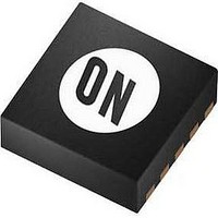
NCV8537MN330R2G ON Semiconductor, NCV8537MN330R2G Datasheet - Page 4

NCV8537MN330R2G
Manufacturer Part Number
NCV8537MN330R2G
Description
Low Dropout (LDO) Regulators LDO
Manufacturer
ON Semiconductor
Datasheet
1.NCV8537MN180R2G.pdf
(16 pages)
Specifications of NCV8537MN330R2G
Number Of Outputs
1
Input Voltage Max
16 V
Output Voltage
3.3 V
Output Type
Fixed
Dropout Voltage (max)
340 mV
Output Current
700 mA
Load Regulation
0.04 mV/mA
Voltage Regulation Accuracy
+/- 0.9 %
Maximum Operating Temperature
+ 125 C
Mounting Style
SMD/SMT
Minimum Operating Temperature
- 40 C
Package / Case
DFN10
Primary Input Voltage
12V
Output Voltage Fixed
3.3V
Dropout Voltage Vdo
340mV
No. Of Pins
10
Voltage Regulator Case Style
DFN
Operating Temperature Range
-40°C To +125°C
Rohs Compliant
Yes
Lead Free Status / RoHS Status
Lead free / RoHS Compliant
Available stocks
Company
Part Number
Manufacturer
Quantity
Price
Company:
Part Number:
NCV8537MN330R2G
Manufacturer:
ON Semiconductor
Quantity:
2 400
Stresses exceeding Maximum Ratings may damage the device. Maximum Ratings are stress ratings only. Functional operation above the
Recommended Operating Conditions is not implied. Extended exposure to stresses above the Recommended Operating Conditions may affect
device reliability.
NOTE:
*Which ever is less. Reverse bias protection feature valid only if (V
1. As mounted on a 35 x 35 x 1.5 mm FR4 Substrate, with a single layer of a specified copper area of 2 oz (0.07 mm thick) copper traces and
PIN FUNCTION DESCRIPTION
MAXIMUM RATINGS
THERMAL CHARACTERISTICS
Input Voltage
Output Voltage
PWRG Pin Voltage
Shutdown Pin Voltage
Junction Temperature Range
Storage Temperature Range
Junction−to−Air, qJA
Junction−to−Pin, J−L4
Pin No.
EPAD
heat spreading area. JEDEC 51 specifications for a low and high conductivity test board recommend a 2 oz copper thickness. Test conditions
are under natural convection or zero air flow.
9, 10
1, 2
3
4
5
6
7
8
This device series contains ESD protection and exceeds the following tests:
Human Body Model (HBM) tested per AEC−Q100−002 (EIA/JESD22−A114)
Machine Model (MM) tested per AEC−Q100−003 (EIA/JESD22−A115)
Charged Device Model (CDM) tested per EIA/JESD22−C101.
SENSE/ADJ
Characteristic
Pin Name
PWRG
EPAD
GND
V
NC
NR
SD
V
out
in
Regulated output voltage. Bypass to ground with C
For output voltage sensing, connect to Pins 1 and 2.at Fixed output Voltage version
Adjustable pin at Adjustable output version
Power Supply Ground
Power Good
Not Connected
Noise Reduction Pin. This is an optional pin used to further reduce noise.
Shutdown pin. When not in use, this pin should be connected to the input pin.
Power Supply Input Voltage
Exposed thermal pad should be connected to ground.
Rating
Min Pad Board (Note 1)
http://onsemi.com
215
58
out
4
− V
Test Conditions (Typical Value)
in
) ≤ 7 V.
Description
out
Symbol
V
PWRG
V
V
T
V
w 1.0 mF
T
out
stg
sh
in
J
1, Pad Board (Note 1)
−0.3 to V
−40 to +150
−50 to +150
−0.3 to +16
−0.3 to +16
−0.3 to +16
in
Value
66
18
+0.3 or 10 V*
Unit
°C
°C
°C/W
°C/W
V
V
V
V
Unit


