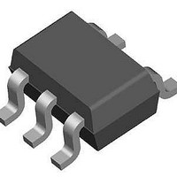
NCP4588DSQ25T1G ON Semiconductor, NCP4588DSQ25T1G Datasheet - Page 3

NCP4588DSQ25T1G
Manufacturer Part Number
NCP4588DSQ25T1G
Description
Low Dropout (LDO) Regulators 200 MA, CAP LESS LV LDO
Manufacturer
ON Semiconductor
Datasheet
1.NCP4588DSQ10T1G.pdf
(17 pages)
Specifications of NCP4588DSQ25T1G
Input Voltage Max
5.25 V
Output Voltage
4.2 V
Dropout Voltage (max)
270 mV
Output Current
400 mA
Load Regulation
25 mV
Voltage Regulation Accuracy
1 %
Maximum Power Dissipation
380 mW
Mounting Style
SMD/SMT
Package / Case
SC-70
Primary Input Voltage
5.25V
Output Voltage Fixed
2.5V
Dropout Voltage Vdo
270mV
No. Of Pins
5
Voltage Regulator Case Style
SC-70
Operating Temperature Range
-40°C To +85°C
Rohs Compliant
Yes
Lead Free Status / RoHS Status
Lead free / RoHS Compliant
Available stocks
Company
Part Number
Manufacturer
Quantity
Price
Company:
Part Number:
NCP4588DSQ25T1G
Manufacturer:
ON
Quantity:
3 000
Company:
Part Number:
NCP4588DSQ25T1G
Manufacturer:
ON Semiconductor
Quantity:
2 200
ELECTRICAL CHARACTERISTICS
−40°C ≤ T
Operating Input Voltage
Output Voltage
Output Voltage Temp.
Coefficient
Line Regulation
Load Regulation
Dropout Voltage
Output Current
Short Current Limit
Quiescent Current
Standby Current
CE Pin Threshold Voltage
CE Pull Down Current
Power Supply Rejection Ratio
Output Noise Voltage
Low Output Nch Tr. On
Resistance
THERMAL CHARACTERISTICS
Thermal Characteristics, XDFN
Thermal Characteristics, SOT23
Thermal Characteristics, SC−70
A
Parameter
Thermal Resistance, Junction−to−Air
Thermal Resistance, Junction−to−Air
Thermal Resistance, Junction−to−Air
≤ 85°C; V
IN
= V
OUT(NOM)
V
V
−40°C ≤ T
OUT
+ 1 V; I
IN
DV
Rating
I
OUT
= V
T
IN
V
= 1 V, I
A
IN
V
OUT
= +25 °C
= 0.2 V
= 200 mA
OUT(NOM)
OUT
= 4 V, V
A
I
+ 1 V or 2.2 V whichever is higher,
OUT
OUT
V
1.2 V < V
≤ 85°C
CE Input Voltage “H”
CE Input Voltage “L”
= 1 mA; C
−40°C ≤ T
CE
Test Conditions
pk−pk
= 1 mA to 200 mA
V
2.2 V ≤ V
= 30 mA, f = 10 Hz to 100 kHz
CE
V
= 0 V, T
OUT
+ 0.5 V ≤ V
OUT
, I
= 0 V, D version only
OUT
OUT
http://onsemi.com
≤ 1.2 V
IN
= 0 V
A
A
1.0 V ≤ V
1.1 V ≤ V
1.2 V ≤ V
1.5 V ≤ V
2.0 V ≤ V
2.6 V ≤ V
≤ 85°C
= 30 mA, f = 1 kHz
= C
OUT
≤ 2.2 V
= 25°C
OUT
V
V
V
V
IN
OUT
OUT
OUT
OUT
≤ 5.0 V
3
= 1 mF; unless otherwise noted. Typical values are at T
OUT
OUT
OUT
OUT
OUT
OUT
> 2.0 V
≤ 2.0 V
> 2.0 V
≤ 2.0 V
< 1.3 V
< 1.5 V
< 1.8 V
< 2.3 V
< 3.0 V
< 4.0 V
Symbol
Symbol
Line
Line
PSRR
R
V
I
R
R
R
V
V
I
CEPD
V
I
V
I
OUT
V
STB
LOW
CEH
OUT
SC
I
CEL
qJA
qJA
qJA
DO
Q
IN
N
Reg
Reg
x0.980
x0.99
Min
−20
−40
200
1.4
1.0
Value
0.02
0.64
0.59
0.55
0.44
0.35
0.27
Typ
250
238
263
9.5
0.1
0.1
100
25
50
70
65
60
80
30
x1.015
x1.01
Max
5.25
0.92
0.84
0.76
0.60
0.49
0.36
0.2
3.0
0.4
20
30
50
25
A
= +25°C.
ppm/°C
mV
°C/W
°C/W
°C/W
Unit
Unit
%/V
mV
mV
mV
mA
mA
dB
mA
mA
mA
W
V
V
V
V
V
rms


