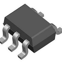
NCP4588DSQ10T1G ON Semiconductor, NCP4588DSQ10T1G Datasheet

NCP4588DSQ10T1G
Specifications of NCP4588DSQ10T1G
Available stocks
Related parts for NCP4588DSQ10T1G
NCP4588DSQ10T1G Summary of contents
Page 1
NCP4588 200 mA, Output Capacitor Free, LDO Linear Voltage Regulator The NCP4588 is a CMOS 200mA LDO which is stable without an output capacitor. This results in a reduction in component count, cost and board area, as well as contributing ...
Page 2
VIN Vref Current Limit CE NCP4588Hxxxxxxx Figure 2. Simplified Schematic Block Diagram PIN FUNCTION DESCRIPTION Pin No. Pin No. Pin No. XDFN SC−70 SOT23 ABSOLUTE ...
Page 3
THERMAL CHARACTERISTICS Rating Thermal Characteristics, XDFN Thermal Resistance, Junction−to−Air Thermal Characteristics, SOT23 Thermal Resistance, Junction−to−Air Thermal Characteristics, SC−70 Thermal Resistance, Junction−to−Air ELECTRICAL CHARACTERISTICS −40°C ≤ T ≤ 85° OUT(NOM) Parameter Operating ...
Page 4
0.6 0.4 0.2 0.0 0 100 200 300 I (mA) OUT Figure 3. Output Voltage vs. Output Current 1.0 V Version (T = 255C) A 3.0 2.5 3.5 V 2.0 ...
Page 5
T , JUNCTION TEMPERATURE (°C) J Figure 9. Output Voltage vs. Temperature, 1.0 V Version 2.55 2.54 2.53 2.52 2.51 2.5 2.49 2.48 2.47 2.46 2.45 −40 −20 0 ...
Page 6
T , JUNCTION TEMPERATURE (°C) J Figure 15. Supply Current vs. Temperature, 1.0 V Version −40 − ...
Page 7
OUT 0.01 0 FREQUENCY (kHz) Figure 21. PSRR, 1.0 V Version, C 100 ...
Page 8
FREQUENCY (kHz) Figure 26. Output Voltage Noise, 2.5 V Version 1.04 1.03 1.02 1.01 1.00 0.99 0.98 0.97 0 1.53 1.52 1.51 1.50 1.49 1.48 ...
Page 9
TYPICAL CHARACTERISTICS 1.53 1.52 1.51 1.50 1.49 1.48 1. 100 120 140 160 180 200 t (ms) Figure 30. Line Transients, 2.5 V Version ms mA, C ...
Page 10
TYPICAL CHARACTERISTICS 1.10 1.05 1.00 0.95 0.90 0. 100 120 140 160 180 200 t (ms) Figure 33. Load Transients, 1.0 V Version 0 ...
Page 11
TYPICAL CHARACTERISTICS 1.90 1.60 1.30 1.00 0.70 0. 100 150 200 250 300 350 400 450 500 t (ms) Figure 36. Load Transients, 1.0 V Version 0 ...
Page 12
TYPICAL CHARACTERISTICS Chip Enable 2.0 1.5 1 OUT 0 200 mA OUT 0.0 −0 100 120 140 160 180 200 t (ms) Figure 39. Start−up, 1.0 V Version, V ...
Page 13
TYPICAL CHARACTERISTICS Chip Enable 2 200 mA OUT 1 OUT 1.0 0 OUT 0.0 −0 (ms) Figure 42. Shutdown, 1.0 V Version ...
Page 14
... ESR may cause unstable output. Enable Operation The enable pin CE may be used for turning the regulator on and off. The regulator is switched on when the CE pin ORDERING INFORMATION Nominal Output Voltage Device NCP4588DSQ10T1G 1.0 V NCP4588DSQ15T1G 1.5 V NCP4588DSQ25T1G 2.5 V NCP4588DMX10TCG 1.0 V NCP4588DMX15TCG 1 ...
Page 15
SC−88A (SC−70−5/SOT−353 −B− 0.2 (0.008 PACKAGE DIMENSIONS CASE 419A−02 ISSUE K NOTES: 1. DIMENSIONING AND TOLERANCING PER ANSI Y14.5M, 1982. 2. CONTROLLING DIMENSION: INCH. 3. ...
Page 16
... SEATING C PLANE 0.22 6X PACKAGE OUTLINE 0.40 PITCH *For additional information on our Pb−Free strategy and soldering details, please download the ON Semiconductor Soldering and Mounting Techniques Reference Manual, SOLDERRM/D. http://onsemi.com 16 ASME Y14.5M, 1994. TERMINAL AND IS MEASURED BETWEEN 0.15 AND 0.25mm FROM TERMINAL TIPS. ...
Page 17
... Opportunity/Affirmative Action Employer. This literature is subject to all applicable copyright laws and is not for resale in any manner. PUBLICATION ORDERING INFORMATION LITERATURE FULFILLMENT: Literature Distribution Center for ON Semiconductor P.O. Box 5163, Denver, Colorado 80217 USA Phone: 303−675−2175 or 800−344−3860 Toll Free USA/Canada Fax: 303− ...


