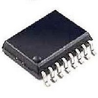
DG408DY-E3 Vishay, DG408DY-E3 Datasheet - Page 12

DG408DY-E3
Manufacturer Part Number
DG408DY-E3
Description
Multiplexer Switch ICs Single 8:1, 3-bit Multiplexer/MUX
Manufacturer
Vishay
Datasheet
1.DG408DY-T1-E3.pdf
(13 pages)
Specifications of DG408DY-E3
Supply Current
0.2 mA
On Resistance (max)
100 Ohms
Propagation Delay Time
180 ns (Typ) @ 12 V
On Time (max)
150 ns
Off Time (max)
150 ns
Supply Voltage (max)
25 V
Maximum Power Dissipation
600 mW
Maximum Operating Temperature
+ 85 C
Minimum Operating Temperature
- 40 C
Package / Case
SOIC-16 Narrow
Mounting Style
SMD/SMT
Number Of Switches
Single
No. Of Circuits
2
On State Resistance Max
40ohm
Supply Voltage Range
± 5V To ± 20V
Operating Temperature Range
-40°C To +85°C
Analog Switch Case Style
SOIC
Lead Free Status / RoHS Status
Lead free / RoHS Compliant
Lead Free Status / RoHS Status
Lead free / RoHS Compliant, Lead free / RoHS Compliant
Available stocks
Company
Part Number
Manufacturer
Quantity
Price
Company:
Part Number:
DG408DY-E3
Manufacturer:
Maxim
Quantity:
1 418
DG408, DG409
Vishay Siliconix
APPLICATION HINTS
Overvoltage Protection
A very convenient form of overvoltage protection consists of
adding two small signal diodes (1N4148, 1N914 type) in
series with the supply pins (see figure 10). This arrangement
effectively blocks the flow of reverse currents. It also floats
the supply pin above or below the normal V+ or V- value. In
this case the overvoltage signal actually becomes the power
Vishay Siliconix maintains worldwide manufacturing capability. Products may be manufactured at one of several qualified locations. Reliability data for Silicon
Technology and Package Reliability represent a composite of all qualified locations. For related documents such as package/tape drawings, part marking, and
reliability data, see www.vishay.com/ppg?70062.
www.vishay.com
12
Enable In
Clock
(MUX On-Off Control)
In
8-Channel Sequential Multiplexer/Demultiplexer
NC
(Outputs)
Analog
Inputs
B
A
DM7493
r
01
IN
IN
+ 15 V
+ 15 V
r
02
GND
Q
Q
Q
Q
B
C
D
A
+ 15 V
S
S
S
S
S
S
S
S
A
NC
V+
1
2
3
4
5
6
7
8
0
A
DG408
GND
Fig. 10 - Overvoltage Protection Using Blocking Diodes
1
A
V
2
- 15 V
g
EN
V-
D
Analog
Output
S
X
(Input)
Reset Enable
Clock
Fig. 11
In
V+
V-
Differential 4-Channel Sequential Multiplexer/Demultiplexer
supply of the IC. From the point of view of the chip, nothing
has changed, as long as the difference VS - (V-) does not
exceed + 44 V. The addition of these diodes will reduce the
analog signal range to 1 V below V+ and 1 V above V-, but it
preserves the low channel resistance and low leakage
characteristics.
1N4148
1N4148
DG408
Differential
(Outputs)
Analog
Inputs
J
CLK
K
CLEAR
1/2 MM74C73
+ 15 V
GND
D
Q
Q
+ 15 V
NC
S
S
S
S
S
S
S
S
V+
1a
2a
3a
4a
1b
2b
3b
4b
A
0
DG409
GND
A
1
J
1/2 MM74C73
CLK
K
- 15 V
S10-1474-Rev. I, 05-Jul-10
EN
Document Number: 70062
V-
CLEAR
D
D
a
b
6
Differential
Q
Q
Outputs
(Inputs)
Analog
NC


