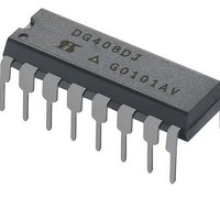
DG408LDY-E3 Vishay, DG408LDY-E3 Datasheet

DG408LDY-E3
Specifications of DG408LDY-E3
Related parts for DG408LDY-E3
DG408LDY-E3 Summary of contents
Page 1
... Portable test equipment • Sample and hold circuits • Communication systems • SDSL, DSLAM • Audio and video signal routing DG409L GND DG408L, DG409L Vishay Siliconix - 17 Ω typ. DS(on ns OFF - 0.2 nA max. S(off) Dual-In- Line, SOIC and TSSOP GND Decoders/Drivers ...
Page 2
... Logic "0" Logic "1" not Care 7 8 and V consult “Digital Control” parameters for specific V+ operation. EN ORDERING INFORMATION DG409L Part Number Temp. Range DG408LDY DG408LDY-E3 DG408LDY-T1 DG408LDY-T1- ° °C DG408LDQ DG408LDQ-E3 DG408LDQ-T1 DG408LDQ-T1-E3 (A Suffix) (D Suffix) c 16-Pin Plastic TSSOP c 16-Pin Narrow SOIC ...
Page 3
... V (DG409L) AX S1b See Figure Ω nF GEN GEN f = 100 kHz kΩ MHz MHz 2 MHz 2 (DG409L only DG408L, DG409L Vishay Siliconix A Suffix D Suffix - 55 °C to 125 ° ° ° Typ. Min. Max. Min. Full Room 17 29 Full 38 Room 1 3 Room 3 7 Room - Full - 15 15 ...
Page 4
... DG408L, DG409L Vishay Siliconix SPECIFICATIONS Dual Supply Parameter Symbol Analog Switch e V Analog Signal Range ANALOG Drain-Source R DS(on) On-Resistance I S(off) Switch Off Leakage a Current I D(off) Channel On Leakage I D(on Current Digital Control V Logic High Input Voltage INH V Logic Low Input Voltage INL ...
Page 5
... V (DG409L) AX S1b Room See Figure 3 Full = 0 Ω Ω nF, R Room L GEN GEN Room f = 100 kHz kΩ L Room MHz Room MHz Room MHz 2 Room (DG409L only) DG408L, DG409L Vishay Siliconix A Suffix D Suffix - 55 °C to 125 ° ° ° Typ. Min. Max. Min. Max 1 ...
Page 6
... DG408L, DG409L Vishay Siliconix SPECIFICATIONS Single Supply 3 V Parameter Symbol Analog Switch e V Analog Signal Range ANALOG Drain-Source R DS(on) On-Resistance I S(off) Switch Off Leakage a Current I D(off) Channel On Leakage I D(on) a Current Digital Control V Logic High Input Voltage INH V Logic Low Input Voltage ...
Page 7
... V+ - Positive Supply Voltage (V) Input Threshold vs. V+ Supply Voltage 125 ° ° ° Drain Voltage ( vs. V and Temperature DS(on) D Document Number: 71342 S09-1259-Rev. F, 13-Jul- ° DG408L, DG409L Vishay Siliconix Drain Voltage ( vs. V and Power Supply DS(on 125 ° ° ° Drain Voltage ( vs. V ...
Page 8
... DG408L, DG409L Vishay Siliconix TYPICAL CHARACTERISTICS 25 °C, unless otherwise noted S(off D(off) I D(on Analog Voltage ( Leakage Current vs. Analog Voltage 1 1000 0.6 0 0.2 0 Source Voltage (V) S Charge Injection vs. Analog Voltage 35 C D(on D(off S(off Drain/Source Capacitance vs. Analog Voltage www.vishay.com OFF 15 10 ...
Page 9
... TEST CIRCUITS Ω DG408L GND V- 300 Ω DG409L GND V- 300 V- Document Number: 71342 S09-1259-Rev. F, 13-Jul-09 Level Decode/ Shift Drive Figure Logic O Input Ω AX Switch Output SB4 Ω Figure 2. Transition Time DG408L, DG409L Vishay Siliconix TRANS (DG408L (DG409L) 4 www.vishay.com 1 n < < TRANS 9 ...
Page 10
... DG408L, DG409L Vishay Siliconix TEST CIRCUITS DG408L GND V- Ω DG409L A 1 GND Ω All S and DG408L A 1 DG409L GND V- Ω www.vishay.com Logic V Input D O Ω 300 V- Switch Output Ω 300 V- Figure 3. Enable Switching Time bbm.5 4 Switch Output Ω 300 35 pF Figure 4. Break-Before-Make Interval t < ...
Page 11
... Insertion Loss = 20 log Figure 8. Insertion Loss Vishay Siliconix maintains worldwide manufacturing capability. Products may be manufactured at one of several qualified locations. Reliability data for Silicon Technology and Package Reliability represent a composite of all qualified locations. For related documents such as package/tape drawings, part marking, and reliability data, see www ...
Page 12
... Vishay product could result in personal injury or death. Customers using or selling Vishay products not expressly indicated for use in such applications their own risk and agree to fully indemnify and hold Vishay and its distributors harmless from and against any and all claims, liabilities, expenses and damages arising or resulting in connection with such use or sale, including attorneys fees, even if such claim alleges that Vishay or its distributor was negligent regarding the design or manufacture of the part ...


