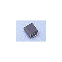
DG419BDQ-T1-E3 Vishay, DG419BDQ-T1-E3 Datasheet - Page 3

DG419BDQ-T1-E3
Manufacturer Part Number
DG419BDQ-T1-E3
Description
Analog Switch ICs Single SPDT 20/25V
Manufacturer
Vishay
Type
Analog Switchr
Specifications of DG419BDQ-T1-E3
Number Of Switches
Single
Switch Configuration
SPDT
On Resistance (max)
35 Ohms @ 12 V
On Time (max)
125 ns @ 12 V
Off Time (max)
66 ns @ 12 V
Off Isolation (typ)
- 82 dB
Supply Voltage (max)
25 V
Supply Current
0.000001 mA @ +/- 16.5 V
Maximum Power Dissipation
400 mW
Maximum Operating Temperature
+ 85 C
Mounting Style
SMD/SMT
Package / Case
MSOP
Minimum Operating Temperature
- 40 C
Off State Leakage Current (max)
12 nA
Propagation Delay Time
87 ns @ +/- 15V/119 ns @ 12V
Analog Switch Type
SPDT
No. Of Channels
1
On State Resistance Max
15ohm
Turn Off Time
38ns
Turn On Time
100ns
Supply Voltage Range
10.8V To 13.2V
Package
8MSOP
Maximum On Resistance
35@10.8V Ohm
Maximum Propagation Delay Bus To Bus
87@±15V|119@12V ns
Maximum High Level Output Current
30 mA
Number Of Channels Per Chip
1
Maximum Turn-off Time
80@±15V ns
Maximum Turn-on Time
125@12V ns
Switch Architecture
SPDT
Power Supply Type
Single|Dual
Lead Free Status / RoHS Status
Lead free / RoHS Compliant
Lead Free Status / RoHS Status
Lead free / RoHS Compliant, Lead free / RoHS Compliant
SCHEMATIC DIAGRAM Typical Channel
Document Number: 70051
S10-1528-Rev. G, 19-Jul-10
SPECIFICATIONS
Parameter
Analog Switch
Analog Signal Range
Drain-Source
On-Resistance
Switch Off Leakage
Current
Channel Off Leakage
Current
Digital Control
Input Current V
Input Current V
Dynamic Characteristics
Turn-On Time
Turn-Off Time
Transition Time
Break-Before-Make
Time Delay (DG403)
Charge Injection
GND
V
V
IN
V+
V-
L
IN
IN
Low
High
e
V
Symbol
a
R
t
ANALOG
TRANS
I
I
I
DS(on)
t
S(off)
D(off)
D(on)
t
OFF
I
I
ON
t
Q
IH
IL
D
V
V+ = 16.5 V, V- = - 16.5 V
S1
C
V+ = 16.5, V- = - 16.5 V
R
R
R
L
Unless Otherwise Specified
L
See Switching Time
L
L
V
V
=
I
= 10 nF, V
V
= 300 , C
= 300 , C
= 300 , C
S
S
S1
V+ = 13.5 V, V- = - 13.5 V
L
±
V
V
= - 10 mA, V
= V
V
V+ = 15 V, V- = - 15 V
= 5 V, V
Test Circuit
D
S
= V
10 V, V
S
Test Conditions
=
=
D
=
S2
±
±
=
±
15.5 V
15.5 V
±
=
gen
10 V
S2
IN
L
L
L
±
15.5 V
= 35 pF
= 35 pF
= 35 pF
Level
Drive
Shift/
= 2.4 V, 0.8 V
=
= 0 V, R
10 V
D
±
=
10 V
±
12.5 V
gen
Figure 1.
DG417
DG418
DG419
DG417
DG418
DG419
DG417
DG418
DG417
DG418
DG419
DG419
= 0
f
Temp.
Room
Room
Room
Room
Room
Room
Room
Room
Room
Room
Room
Full
Full
Full
Full
Full
Full
Full
Full
Full
Full
Full
Full
b
0.005
0.005
Typ.
- 0.1
- 0.1
- 0.1
- 0.4
- 0.4
100
20
60
13
60
DG417, DG418, DG419
c
- 55 °C to 125 °C
Min.
- 0.25
- 0.25
- 0.75
- 0.75
- 0.4
- 0.5
- 0.5
- 15
- 20
- 20
- 60
- 40
- 60
5
A Suffix
d
Max.
0.25
0.25
0.75
0.75
175
250
145
210
175
250
0.4
0.5
0.5
15
35
45
20
20
60
40
60
Vishay Siliconix
d
- 40 °C to 85 °C
- 0.25
- 0.25
- 0.75
- 0.75
Min.
- 0.4
- 0.5
- 0.5
- 15
- 12
- 10
- 12
- 5
- 5
5
V+
V-
D Suffix
d
www.vishay.com
Max.
0.25
0.25
0.75
0.75
175
250
145
210
175
250
0.4
0.5
0.5
15
35
45
12
10
12
S
D
5
5
d
Unit
µA
pC
nA
ns
V
3


