DG442DY-E3 Vishay, DG442DY-E3 Datasheet
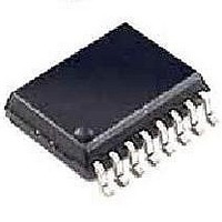
Analog Switch ICs SPST Analog Switch

DG442DY-E3

Manufacturer Part Number
DG442DY-E3
Description
Analog Switch ICs SPST Analog Switch
Manufacturer
Vishay
Type
Analog Switchr
Datasheet

Specifications of DG442DY-E3

Number Of Switches
Quad
Switch Configuration
SPST
On Resistance (max)
160 Ohms
On Time (max)
450 ns
Off Time (max)
200 ns
Supply Voltage (max)
25 V
Supply Current
0.015 mA
Maximum Power Dissipation
900 mW
Maximum Operating Temperature
+ 85 C
Mounting Style
SMD/SMT
Package / Case
SOIC-16 Narrow
Minimum Operating Temperature
- 40 C
Analog Switch Type
SPST
No. Of Channels
4
On State Resistance Max
85ohm
Turn Off Time
110ns
Turn On Time
150ns
Supply Voltage Range
10.8V To 13.2V
Multiplexer Configuration
Quad SPST
Number Of Inputs
4
Number Of Outputs
4
Number Of Channels
4
Analog Switch On Resistance
160@10.8VOhm
Power Supply Requirement
Single/Dual
Single Supply Voltage (min)
13V
Single Supply Voltage (typ)
15/18/24/28V
Single Supply Voltage (max)
36V
Dual Supply Voltage (min)
±7V
Dual Supply Voltage (typ)
±9/±12/±15/±18V
Dual Supply Voltage (max)
±22V
Power Dissipation
900mW
Mounting
Surface Mount
Pin Count
16
Operating Temp Range
-40C to 85C
Operating Temperature Classification
Industrial
Package
16SOIC N
Maximum On Resistance
160@10.8V Ohm
Maximum High Level Output Current
30 mA
Maximum Turn-off Time
210@±15V ns
Maximum Turn-on Time
450@12V ns
Switch Architecture
SPST
Power Supply Type
Single|Dual
Lead Free Status / RoHS Status
Lead free / RoHS Compliant
Lead Free Status / RoHS Status
Lead free / RoHS Compliant, Lead free / RoHS Compliant
DESCRIPTION
The DG441/442 monolithic quad analog switches are
designed to provide high speed, low error switching of
analog and audio signals. The DG441 has a normally closed
function. The DG442 has a normally open function.
Combining low on-resistance (50 Ω, typ.) with high speed
(t
upgrading DG201A/202 sockets. Charge injection has been
minimized on the drain for use in sample-and-hold circuits.
To achieve high voltage ratings and superior switching
performance, the DG441/442 are built on Vishay Siliconix’s
high-voltage silicon-gate process. An epitaxial layer
prevents latchup.
Each switch conducts equally well in both directions when
on, and blocks input voltages to the supply levels when off.
FUNCTIONAL BLOCK DIAGRAM AND PIN CONFIGURATION
* Pb containing terminations are not RoHS compliant, exemptions may apply
Document Number: 70053
S-71241–Rev. I, 25-Jun-07
ON
150 ns, typ.), the DG441/442 are ideally suited for
GND
IN
IN
D
V-
D
S
S
1
1
1
4
4
4
1
2
3
4
5
6
7
8
Dual-In-Line and SOIC
Top View
DG441
Quad SPST CMOS Analog Switches
16
15
14
13
12
10
11
9
IN
D
S
V+
NC
S
D
IN
2
3
2
3
2
3
FEATURES
BENEFITS
APPLICATIONS
Logic "0" ≤ 0.8 V
Logic "1" ≥ 2.4 V
• Low On-Resistance: 50 Ω
• Low Leakage: 80 pA
• Low Power Consumption: 0.2 mW
• Fast Switching Action-t
• Low Charge Injection-Q: - 1 pC
• DG201A/DG202 Upgrades
• TTL/CMOS-Compatible Logic
• Single Supply Capability
• Less Signal Errors and Distortion
• Reduced Power Supply Requirements
• Faster Throughput
• Improved Reliability
• Reduced Pedestal Errors
• Simplifies Retrofit
• Simple Interfacing
• Audio Switching
• Battery Powered Systems
• Data Acquisition
• Hi-Rel Systems
• Sample-and-Hold Circuits
• Communication Systems
• Automatic Test Equipment
• Medical Instruments
GND
TRUTH TABLE
NC
V-
S
S
1
4
Key
Logic
4
5
6
7
8
0
1
3
9
D
D
1
4
10
2
IN
IN
1
4
Top View
DG441
11
1
LCC
NC
NC
20
12
ON
DG441
IN
IN
OFF
ON
2
3
: 150 ns
19
13
D
D
2
3
Vishay Siliconix
18
17
16
15
14
DG441/442
S
V+
NC
NC
S
2
3
www.vishay.com
DG442
OFF
ON
RoHS*
COMPLIANT
Available
Pb-free
1

Related parts for DG442DY-E3

DG442DY-E3 Summary of contents

Page 1

... DG201A/202 sockets. Charge injection has been minimized on the drain for use in sample-and-hold circuits. To achieve high voltage ratings and superior switching performance, the DG441/442 are built on Vishay Siliconix’s high-voltage silicon-gate process. An epitaxial layer prevents latchup. Each switch conducts equally well in both directions when on, and blocks input voltages to the supply levels when off ...

Page 2

... Narrow SOIC Level Shift/ Drive Figure 1. Part Number DG441DJ DG441DJ-E3 DG442DJ DG442DJ-E3 DG441DY DG441DY-E3 DG441DY-T1 DG441DY-T1-E3 DG442DY DG442DY-E3 DG442DY-T1 DG442DY-T1-E3 Limit mA, whichever occurs first 30 100 - 65 to 150 - 65 to 125 450 900 900 1200 V- V+ Document Number: 70053 S-71241–Rev. I, 25-Jun-07 ...

Page 3

... Ω gen gen = 50 Ω MHz TALK S(off MHz D(off D(on) ANALOG 16 16 DG441/442 Vishay Siliconix A Suffix D Suffix - 55 to 125 ° ° Temp Typ Min Max Min Full - Room 50 85 Full 100 Room 4 Full 5 ± Room 0.01 - 0.5 0.5 - 0.5 Full ...

Page 4

... DG441/442 Vishay Siliconix a SPECIFICATIONS FOR SINGLE SUPPLY Parameter Symbol Analog Switch e V Analog Signal Range ANALOG Drain-Source r DS(on) On-Resistance Dynamic Characteristics t Turn-On Time ON t Turn-Off Time OFF Charge Injection Q Power Supplies Positive Supply Current I+ Negative Supply Current I- I Ground Current GND Notes: a ...

Page 5

... Frequency (Hz) Crosstalk and Off Isolation vs. Frequency Document Number: 70053 S-71241–Rev. I, 25-Jun-07 ± ± ± ± ± ± Crosstalk Off Isolation 100 DG441/442 Vishay Siliconix 125 ° ° ° °C 0 ° ° – Drain Voltage ( vs. V and Temperature DS(on) ...

Page 6

... DG441/442 Vishay Siliconix TYPICAL CHARACTERISTICS 25 °C, unless otherwise noted 2.4 1.6 0.8 0 ± 5 ± V+, V– Positive and Negative Supplies (V) Switching Threshold vs. Supply Voltage S(off) D(off S(on) D(on – Drain or Source Voltage ( Source/Drain Leakage Currents (Single 12 V Supply) 160 140 t ON ...

Page 7

... Document Number: 70053 S-71241–Rev. I, 25-Jun-07 Logic Input V O Switch C Input Switch Output Figure 2. Switching Time Figure 3. Charge Injection Ω GND Figure 6. Source/Drain Capacitances DG441/442 Vishay Siliconix < < OFF Note: Logic input waveform is inverted for DG442 OFF ON (DG441) OFF Δ (DG442 Ω ...

Page 8

... V Figure 9. Precision-Weighted Resistor Programmable-Gain Amplifier Vishay Siliconix maintains worldwide manufacturing capability. Products may be manufactured at one of several qualified locations. Reliability data for Silicon Technology and Package Reliability represent a composite of all qualified locations. For related documents such as package/tape drawings, part marking, and reliability data, see http://www.vishay.com/ppg?70053. ...

Page 9

... Vishay disclaims any and all liability arising out of the use or application of any product described herein or of any information provided herein to the maximum extent permitted by law. The product specifications do not expand or otherwise modify Vishay’ ...

Related keywords