FP31QF-F TriQuint, FP31QF-F Datasheet

RF Mixer 50-4000MHz +34dBm P1dB

FP31QF-F

Manufacturer Part Number
FP31QF-F
Description
RF Mixer 50-4000MHz +34dBm P1dB
Manufacturer
TriQuint
Datasheet

Specifications of FP31QF-F

Frequency Range
915 MHz to 2450 MHz
Mounting Style
SMD/SMT
Operating Supply Voltage
9 V
Supply Current
450 mA
Package / Case
QFN
Noise Figure
3.5 dB
Lead Free Status / RoHS Status
Lead free / RoHS Compliant
Other names
1066886

Available stocks

Company
Part Number
Manufacturer
Quantity
Price
Part Number:
FP31QF-F
Manufacturer:
WJ
Quantity:
12 800
Part Number:
FP31QF-F
Manufacturer:
WJ
Quantity:
20 000
Product Features
Applications
Specifications
1. Pinch-off voltage is measured when I
2. Test conditions unless otherwise noted: T = 25 ºC, V
3. 3OIP measured with two tones at an output power of +18 dBm/tone separated by 1 MHz. The
Absolute Maximum Rating
Operation of this device above any of these parameters may cause permanent damage.
WJ Communications, Inc • Phone 1-800-WJ1-4401 • FAX: 408-577-6621 • e-mail: sales@wj.com • Web site: www.wj.com, www.TriQuint.com
DC Parameter
Saturated Drain Current, I
Transconductance, G
Pinch Off Voltage, V
RF Parameter
Operational Bandwidth
Test Frequency
Small Signal Gain
Maximum Stable Gain
Output P1dB
Output IP3
Noise Figure
Parameter
Storage Temperature
DC Power
RF Input Power (continuous)
Drain to Gate Voltage, V
Thermal Resistance, Rth
Junction Temperature
50 – 4000 MHz
18 dB Gain @ 900 MHz
+34 dBm P1dB
+46 dBm Output IP3
High Drain Efficiency
Single Voltage Supply
Robust 1000V ESD, Class IC
Lead free/green/RoHS-compliant
6mm 28-pin QFN package
Mobile Infrastructure
CATV / DBS
W-LAN / ISM
RFID
Defense / Homeland Security
Fixed Wireless
application circuit with Z
suppression on the largest IM3 product is used to calculate the 3OIP using a 2:1 rule.
(3)
FP31QF
2-Watt HFET
L
= Z
(2)
m
p
LOPT
(1)
dss
, Z
dg
ds
S
= Z
= 4.8 mA.
SOPT
(optimized for output power).
Units Min
Units Min
MHz
MHz
dBm
dBm
mA
mS
dB
dB
dB
V
DS
= 9 V, I
Rating
-55 to +125 °C
7.5 W
6 dB above Input P1dB
+16 V
18°C/W
+160°C
The FP31QF is a high performance 2-Watt HFET
(Heterostructure FET) in a low-cost lead-free/RoHS-
compliant 28-pin 6x6 mm QFN (Quad Flatpack, No-
Lead) surface-mount package.
optimally at a drain bias of +9 V and 450 mA to achieve
+46 dBm output IP3 performance and an output power of
+34 dBm at 1-dB compression.
The device conforms to WJ Communications’ long
history of producing high reliability and quality
components. The FP31QF has an associated MTTF of a
minimum of 100 years at a mounting temperature of
85°C. All devices are 100% RF & DC tested.
The product is targeted for use as driver amplifiers for
wireless infrastructure where high performance and high
efficiency are required.
DQ
50
= 450 mA, in a tuned
Product Description
Typ Max
Typ Max
1170
590
-2.0
+34
+46
800
3.5
18
24
4000
Typical Performance
4. Typical parameters represent performance in an application circuit.
5. Empirical measurements showed optimal power performance at a drain voltage = 9 volts at 450 mA.
Ordering Information
Standard tape / reel size = 500 pieces on a 7” reel
Parameter
Frequency
Gain
S11
S22
Output P1dB
Output IP3
Noise Figure
IS-95 Channel Power
W-CDMA Ch. Power
Drain Voltage
Drain Current
Part No.
FP31QF-F
FP31QF-PCB900
FP31QF-PCB1900
FP31QF-PCB2140
Because the FP31QF is a discrete device, users can choose their own bias configuration. Performance
may vary from the data shown depending on the biasing conditions. To achieve a minimum 1 million
hours MTTF rating, the biasing condition should maintain a junction temperature below 160 °C over all
operating temperatures. This can be approximated by (drain voltage) x (drain current) x 17.5 °C/W +
(maximum operating temperature).
@ -45 dBc ACPR
@ -45 dBc ACLR
This device works
(3)
(5)
(5)
Specifications and information are subject to change without notice
Description
2-Watt HFET
(lead-free/RoHS-compliant 6mm QFN package)
870 – 960 MHz Application Circuit
1930 – 1990 MHz Application Circuit
2110 – 2170 MHz Application Circuit
Units
MHz
dBm
dBm
dBm
dBm
mA
dB
dB
dB
dB
V
GATE /
Functional Diagram
RF IN
GND
GND
GND
GND
GND
GND
+27.8
1
2
3
4
5
6
7
+34
+46
915
-20
-12
3.5
18
RF Output
Function
RF Input
(4)
Ground
Drain /
28
Gate /
8
27
9
+33.8 +33.2 +33.5
+46.8 +46.6 +46.8
+27.3
1960
13.5
Typical
-20
-11
26
10
4.5
450
Page 1 of 12 March 2008
25
11
+9
All other pins &
backside copper
24
12
2140
+25
-18
-24
4.6
13
Pin No.
23
13
19
3
22
14
2450
-18
-15
4.6
12
21
20
19
18
17
16
15
GND
GND
DRAIN /
RF OUT
GND
GND
GND
GND

Related parts for FP31QF-F

FP31QF-F Summary of contents

Page 1

... MTTF rating, the biasing condition should maintain a junction temperature below 160 °C over all operating temperatures. This can be approximated by (drain voltage) x (drain current) x 17.5 °C/W + (maximum operating temperature). Ordering Information Part No. FP31QF-F FP31QF-PCB900 FP31QF-PCB1900 FP31QF-PCB2140 Standard tape / reel size = 500 pieces on a 7” reel ...

Page 2

... FP31QF 2-Watt HFET S-Parameters (V S21, Maximum Stable Gain vs. Frequency DB(|S[2,1]|) DB(MSG 0.5 1 1.5 2 Frequency (GHz) Note: Measurements were made on the packaged device in a test fixture with 50 ohm input and output lines. The S-parameters shown are the de-embedded data down to the device leads and represents typical performance of the device. ...

Page 3

... The C2 and C3 placements are at silk screen markers, “H” and “9.5”, respectively. • The via hole spacing along the main microstrip line is .040”. • The distance from the edge of the FP31QF to the closer edge .305”. • The transmission line lengths shown in the schematic are from the FP31QF device edge to the component edge ...

Page 4

... FP31QF 2-Watt HFET FP31QF-PCB900 Application Circuit Performance Plots S11 vs. Frequency 0 -40c +25c +85c -5 -10 -15 -20 -25 -30 860 880 900 920 940 Frequency (MHz) P1dB vs. Frequency -40c +25c +85c 26 860 880 900 920 940 Frequency (MHz) OIP3 vs. Temperature freq = 915, 916 MHz ...

Page 5

... The C2 and C3 placements are at silk screen markers, “B” and “3”, respectively. • The via hole spacing along the main microstrip line is .040”. • The distance from the edge of the FP31QF to the closer edge .305”. • The transmission line lengths shown in the schematic are from the FP31QF device edge to the component edge ...

Page 6

... FP31QF 2-Watt HFET FP31QF-PCB1900 Application Circuit Performance Plots S11 vs. Frequency 0 -40C +25C +85C -5 -10 -15 -20 -25 -30 1930 1950 1970 Frequency (MHz) P1dB vs. Frequency -40c +25c +85c 26 1930 1950 1970 Frequency (MHz) OIP3 vs. Temperature freq = 1960, 1961 MHz 42 +18 dBm / tone 40 -40 ...

Page 7

... The C2 and C3 placements are at silk screen markers, “A” and “2.5”, respectively. • The via hole spacing along the main microstrip line is .040”. • The distance from the edge of the FP31QF to the closer edge .305”. • The transmission line lengths shown in the schematic are from the FP31QF device edge to the component edge ...

Page 8

... FP31QF 2-Watt HFET FP31QF-PCB2140 Application Circuit Performance Plots S11 vs. Frequency 0 -40c +25c +85c -5 -10 -15 -20 -25 -30 2110 2130 2150 2170 Frequency (MHz) P1dB vs. Frequency -40C +25C +85C 26 2110 2130 2150 2170 Frequency (MHz) OIP3 vs. Temperature freq = 2140, 2141 MHz 42 +18 dBm / tone ...

Page 9

... The C2 and C3 placements are at silk screen markers, “A” and “2”, respectively. • The via hole spacing along the main microstrip line is .040”. • The distance from the edge of the FP31QF to the closer edge .305”. • The transmission line lengths shown in the schematic are from the FP31QF device edge to the component edge ...

Page 10

... The via hole spacing along the main microstrip line is .040”. • The distance from the edge of the FP31QF to the closer edge .305”. • The transmission line lengths shown in the schematic are from the FP31QF device edge to the component edge ...

Page 11

... The active-bias circuit, shown on the right, uses dual PNP transistors to provide a constant drain current into the FP31QF, while also eliminating the effects of pinchoff variation. This configuration is best suited for applications where the intended output power level of the amplifier is backed off at least 6 dB away from its compression point ...

Page 12

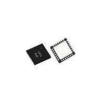
... FP31QF 2-Watt HFET FP31QF-F Mechanical Information This package is lead-free/RoHS-compliant compatible with both lead-free (maximum 260 °C reflow temperature) and leaded (maximum 245 °C reflow temperature) soldering processes. The plating material on the pins is annealed matte tin over copper. Outline Drawing Mounting Configuration / Land Pattern WJ Communications, Inc • ...

Related keywords