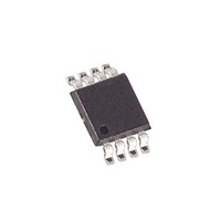
MAX9933EUA+ Maxim Integrated Products, MAX9933EUA+ Datasheet - Page 11

MAX9933EUA+
Manufacturer Part Number
MAX9933EUA+
Description
RF Detector 2MHZ-1.6GHZ RF-DETCT CONTLR & RF DETECTOR
Manufacturer
Maxim Integrated Products
Datasheet
1.MAX9933EUA.pdf
(16 pages)
Specifications of MAX9933EUA+
Maximum Operating Temperature
+ 85 C
Minimum Operating Temperature
- 40 C
Mounting Style
SMD/SMT
Package / Case
uMAX
Lead Free Status / RoHS Status
Lead free / RoHS Compliant
The MAX9930–MAX9933 family of logarithmic ampli-
fiers (log amps) comprises four main amplifier/limiter
stages each with a small-signal gain of 10dB. The out-
put stage of each amplifier is applied to a full-wave rec-
tifier (detector). A detector stage also precedes the first
gain stage. In total, five detectors, each separated by
10dB, comprise the log amp strip. Figure 1 shows the
functional diagram of the log amps.
A portion of the PA output power is coupled to RFIN of
the logarithmic amplifier controller/detector, and is
applied to the logarithmic amplifier strip. Each detector
cell outputs a rectified current and all cell currents are
summed and form a logarithmic output. The detected
output is applied to a high-gain g
buffered and then applied to OUT. For the
MAX9930/MAX9931/MAX9932, OUT is applied to the
gain-control input of the PA to close the control loop.
The voltage applied to SET determines the output
power of the PA in the control loop. The voltage applied
to SET relates to an input power level determined by
the log amp detector characteristics. For the MAX9933,
OUT is applied to an ADC typically found in a base-
band IC which, in turn, controls the PA biasing with the
output (Figure 2).
Figure 2. MAX9933 Typical Application Circuit
50Ω
50Ω
XX
C
CLPF
C
C
______________________________________________________________________________________
______________________________________________________________________________________
RFIN
SHDN
GND
CLPF
Detailed Description
MAX9933
PA
2MHz to 1.6GHz 45dB RF-Detecting
GND
OUT
N.C.
TRANSMITTER
V
CC
m
V
CC
stage, which is
0.01µF
DAC
ADC
BASEBAND
Controllers and RF Detector
IC
Extrapolating a straight-line fit of the graph of SET vs.
RFIN provides the logarithmic intercept. Logarithmic
slope, the amount SET changes for each dB change of
RF input, is generally independent of waveform or termi-
nation impedance. The MAX9930/MAX9931/MAX9932
slope at low frequencies is about 25mV/dB.
Variance in temperature and supply voltage does not
alter the slope significantly as shown in the Typical
Operating Characteristics .
The MAX9930/MAX9931/MAX9932 are specifically
designed for use in PA control applications. In a control
loop, the output starts at approximately 2.9V (with supply
voltage of 3V) for the minimum input signal and falls to a
value close to ground at the maximum input. With a por-
tion of the PA output power coupled to RFIN, apply a volt-
age to SET (for the MAX9930/MAX9931/MAX9932) and
connect OUT to the gain-control pin of the PA to control
its output power. An external capacitor from CLPF to
ground sets the bandwidth of the PA control loop.
Logarithmic slope and intercept determine the transfer
function of the MAX9930–MAX9933 family of log amps.
The change in SET voltage (OUT voltage for the
MAX9933) per dB change in RF input defines the loga-
rithmic slope. Therefore, a 10dB change in RF input
results in a 250mV change at SET (OUT for the
MAX9933). The Log Conformance vs. Input Power plots
(see Typical Operating Characteristics ) show the dynam-
ic range of the log amp family. Dynamic range is the
range for which the error remains within a band of ±1dB.
The intercept is defined as the point where the linear
response, when extrapolated, intersects the y-axis of
the Log Conformance vs. Input Power plot. Using these
parameters, the input power can be calculated at any SET
voltage level (OUT voltage level for the MAX9933) within
the specified input range with the following equations:
where SET is the set-point voltage, OUT is the output
voltage for the MAX9933, SLOPE is the logarithmic slope
(V/dB), RFIN is in either dBm or dBV and IP is the loga-
rithmic intercept point utilizing the same units as RFIN.
(MAX9930/MAX9931/MAX9932)
(MAX9933)
RFIN = (SET / SLOPE) + IP
RFIN = (OUT / SLOPE) + IP
Transfer Function
11
11


