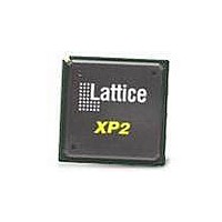
LFXP2-30E-5FN484C Lattice, LFXP2-30E-5FN484C Datasheet - Page 53

LFXP2-30E-5FN484C
Manufacturer Part Number
LFXP2-30E-5FN484C
Description
FPGA - Field Programmable Gate Array 30KLUTs 363 I/O Inst -on DSP 1.2V -5 Spd
Manufacturer
Lattice
Specifications of LFXP2-30E-5FN484C
Number Of Macrocells
29000
Number Of Programmable I/os
363
Data Ram Size
396288
Supply Voltage (max)
1.26 V
Maximum Operating Temperature
+ 85 C
Minimum Operating Temperature
0 C
Mounting Style
SMD/SMT
Supply Voltage (min)
1.14 V
Package / Case
FPBGA-484
Lead Free Status / RoHS Status
Lead free / RoHS Compliant
Available stocks
Company
Part Number
Manufacturer
Quantity
Price
Company:
Part Number:
LFXP2-30E-5FN484C
Manufacturer:
Lattice Semiconductor Corporation
Quantity:
10 000
Lattice Semiconductor
Table 3-1. LVDS25E DC Conditions
LVCMOS33D
All I/O banks support emulated differential I/O using the LVCMOS33D I/O type. This option, along with the external
resistor network, provides the system designer the flexibility to place differential outputs on an I/O bank with 3.3V
VCCIO. The default drive current for LVCMOS33D output is 12mA with the option to change the device strength to
4mA, 8mA, 16mA or 20mA. Follow the LVCMOS33 specifications for the DC characteristics of the LVCMOS33D.
V
Z
R
R
R
V
V
V
V
Z
I
DC
Parameter
OUT
OH
OL
OD
BACK
CCIO
T
CM
S
P
Output Driver Supply (+/-5%)
Driver Impedance
Driver Series Resistor (+/-1%)
Driver Parallel Resistor (+/-1%)
Receiver Termination (+/-1%)
Output High Voltage (after R
Output Low Voltage (after R
Output Differential Voltage (After R
Output Common Mode Voltage
Back Impedance
DC Output Current
Description
P
P
3-9
)
)
P
)
Typical
DC and Switching Characteristics
100.5
2.50
1.43
1.07
0.35
1.25
6.03
158
140
100
20
LatticeXP2 Family Data Sheet
Units
mA
V
V
V
V
V


