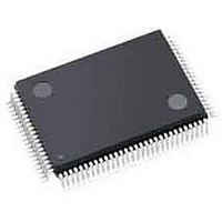
APA075-TQG100 Actel, APA075-TQG100 Datasheet - Page 13

APA075-TQG100
Manufacturer Part Number
APA075-TQG100
Description
FPGA - Field Programmable Gate Array 75K System Gates
Manufacturer
Actel
Datasheet
1.APA075-FGG144.pdf
(178 pages)
Specifications of APA075-TQG100
Processor Series
APA075
Core
IP Core
Maximum Operating Frequency
150 MHz
Number Of Programmable I/os
158
Data Ram Size
27648
Supply Voltage (max)
2.7 V
Maximum Operating Temperature
+ 70 C
Minimum Operating Temperature
0 C
Development Tools By Supplier
APA-Eval-Kit, APA-Eval-BRD1, Silicon-Explorer II, Silicon-Sculptor 3, SI-EX-TCA, Flashpro 4, Flashpro 3, Flashpro Lite
Mounting Style
SMD/SMT
Supply Voltage (min)
2.3 V
Number Of Gates
75 K
Package / Case
TQFP-100
Lead Free Status / RoHS Status
Lead free / RoHS Compliant
Available stocks
Company
Part Number
Manufacturer
Quantity
Price
Part Number:
APA075-TQG100
Manufacturer:
ACTEL
Quantity:
20 000
Company:
Part Number:
APA075-TQG100A
Manufacturer:
Microsemi SoC
Quantity:
10 000
Company:
Part Number:
APA075-TQG100I
Manufacturer:
Microsemi SoC
Quantity:
10 000
Part Number:
APA075-TQG100I
Manufacturer:
ACTEL/爱特
Quantity:
20 000
Figure 2-3 • High-Speed, Very Long-Line Resources
Clock Resources
The ProASIC
control of circuit timing through the use of analog
circuitry. Each chip has two clock conditioning blocks
containing a phase-locked loop (PLL) core, delay lines,
phase shifter (0
all
interconnection of inputs to the global network (thus
providing bidirectional access to the PLL). This permits
the PLL block to drive inputs and/or outputs via the two
global lines on each side of the chip (four total lines).
This circuitry is discussed in more detail in the
"ProASIC
page
the
2-10.
PLUS
circuitry
PLUS
Clock Management System" section on
°
and 180
PAD RING
family offers powerful and flexible
needed
°
), clock multiplier/dividers, and
High-Speed Very Long-Line Resouces
for
the
selection
and
PAD RING
v5.9
Clock Trees
One of the main architectural benefits of ProASIC
the set of power- and delay-friendly global networks.
ProASIC
is based on a network of spines and ribs that reach all
the tiles in their regions
flexible clock tree architecture allows users to map up to
88 different internal/external clocks in an APA1000
device. Details on the clock spines and various numbers
of the family are given in
The flexible use of the ProASIC
designer to cope with several design requirements. Users
implementing clock-resource intensive applications can
easily route external or gated internal clocks using global
routing spines. Users can also drastically reduce delay
penalties and save buffering resources by mapping
critical high fanout nets to spines. For design hints on
using these features, refer to Actel’s
ProASIC Clock Trees
PLUS
offers four global trees. Each of these trees
application note.
ProASIC
Table 2-1 on page
(Figure 2-4 on page
PLUS
PLUS
clock spine allows the
Flash Family FPGAs
SRAM
SRAM
Efficient Use of
2-4.
2-4). This
PLUS
2-3
is


