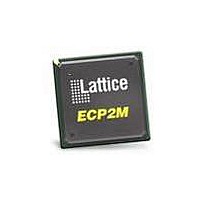
LFE2-6E-7FN256C Lattice, LFE2-6E-7FN256C Datasheet - Page 47

LFE2-6E-7FN256C
Manufacturer Part Number
LFE2-6E-7FN256C
Description
FPGA - Field Programmable Gate Array 6K LUTs 190 I/O DSP 1.2V -7
Manufacturer
Lattice
Datasheet
1.LFE2-12SE-6FN256C.pdf
(389 pages)
Specifications of LFE2-6E-7FN256C
Number Of Macrocells
6000
Number Of Programmable I/os
190
Data Ram Size
56320
Supply Voltage (max)
1.26 V
Maximum Operating Temperature
+ 85 C
Minimum Operating Temperature
0 C
Mounting Style
SMD/SMT
Supply Voltage (min)
1.14 V
Package / Case
FPBGA-256
Lead Free Status / RoHS Status
Lead free / RoHS Compliant
Available stocks
Company
Part Number
Manufacturer
Quantity
Price
Company:
Part Number:
LFE2-6E-7FN256C
Manufacturer:
LATTICE
Quantity:
279
Company:
Part Number:
LFE2-6E-7FN256C
Manufacturer:
Lattice Semiconductor Corporation
Quantity:
10 000
Company:
Part Number:
LFE2-6E-7FN256C-6I
Manufacturer:
ZARLINK
Quantity:
7 000
- Current page: 47 of 389
- Download datasheet (5Mb)
Lattice Semiconductor
O standards (together with their supply and reference voltages) supported by LatticeECP2/M devices. For further
information about utilizing the sysI/O buffer to support a variety of standards please see the the list of additional
technical information at the end of this data sheet.
Table 2-13. Supported Input Standards
Single Ended Interfaces
LVTTL
LVCMOS33
LVCMOS25
LVCMOS18
LVCMOS15
LVCMOS12
PCI 33
HSTL18 Class I, II
HSTL15 Class I
SSTL3 Class I, II
SSTL2 Class I, II
SSTL18 Class I, II
Differential Interfaces
Differential SSTL18 Class I, II
Differential SSTL2 Class I, II
Differential SSTL3 Class I, II
Differential HSTL15 Class I
Differential HSTL18 Class I, II
LVDS, MLVDS, LVPECL, BLVDS, RSDS
1 When not specified, V
Input Standard
CCIO
can be set anywhere in the valid operating range (page 3-1).
V
2-44
REF
0.75
1.25
0.9
1.5
0.9
—
—
—
—
—
—
—
—
—
—
—
—
—
(Nom.)
LatticeECP2/M Family Data Sheet
V
CCIO
1.8
1.5
3.3
1
—
—
—
—
—
—
—
—
—
—
—
—
—
—
—
(Nom.)
Architecture
Related parts for LFE2-6E-7FN256C
Image
Part Number
Description
Manufacturer
Datasheet
Request
R

Part Number:
Description:
FPGA - Field Programmable Gate Array 6K LUTs 90 I/O DSP 1.2V -7
Manufacturer:
Lattice
Datasheet:

Part Number:
Description:
FPGA - Field Programmable Gate Array 6K LUTs 190 I/O DSP 1.2V -7
Manufacturer:
Lattice
Datasheet:

Part Number:
Description:
FPGA - Field Programmable Gate Array 6K LUTs 190 I/O DSP 1.2V -5
Manufacturer:
Lattice
Datasheet:

Part Number:
Description:
FPGA - Field Programmable Gate Array 6K LUTs 90 I/O DSP 1.2V -5
Manufacturer:
Lattice
Datasheet:

Part Number:
Description:
FPGA - Field Programmable Gate Array 6K LUTs 190 I/O DSP 1.2V -6
Manufacturer:
Lattice
Datasheet:

Part Number:
Description:
IC, LATTICEECP2 FPGA, 420MHZ, TQFP-144
Manufacturer:
LATTICE SEMICONDUCTOR
Datasheet:
Part Number:
Description:
FPGA LatticeECP2 Family 6000 Cells 90nm (CMOS) Technology 1.2V 256-Pin FBGA
Manufacturer:
LATTICE SEMICONDUCTOR
Datasheet:
Part Number:
Description:
FPGA LatticeECP2 Family 6000 Cells 90nm (CMOS) Technology 1.2V 144-Pin TQFP
Manufacturer:
LATTICE SEMICONDUCTOR
Datasheet:

Part Number:
Description:
IC FPGA 6KLUTS 90I/O 144-TQFP
Manufacturer:
Lattice
Datasheet:

Part Number:
Description:
IC FPGA 6KLUTS 90I/O 144-TQFP
Manufacturer:
Lattice
Datasheet:

Part Number:
Description:
IC FPGA 6KLUTS 190I/O 256-BGA
Manufacturer:
Lattice
Datasheet:

Part Number:
Description:
IC FPGA 6KLUTS 190I/O 256-BGA
Manufacturer:
Lattice
Datasheet:

Part Number:
Description:
IC FPGA 6KLUTS 190I/O 256-BGA
Manufacturer:
Lattice
Datasheet:

Part Number:
Description:
IC FPGA 6KLUTS 190I/O 256-BGA
Manufacturer:
Lattice
Datasheet:

Part Number:
Description:
FPGA - Field Programmable Gate Array 6K LUTs 90 I/O DSP 1.2V -5 I
Manufacturer:
Lattice
Datasheet:


