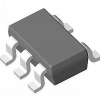
AAT4900IGV-T1 Analogic Tech, AAT4900IGV-T1 Datasheet - Page 8

AAT4900IGV-T1
Manufacturer Part Number
AAT4900IGV-T1
Description
MOSFET & Power Driver ICs Buffered Power Half-Bridge
Manufacturer
Analogic Tech
Type
Buffered Power Half-Bridger
Datasheet
1.AAT4900IGV-T1.pdf
(13 pages)
Specifications of AAT4900IGV-T1
Product
Half-Bridge Drivers
Rise Time
5 ns
Fall Time
5 ns
Supply Voltage (max)
6 V
Supply Voltage (min)
- 0.3 V
Supply Current
4 mA
Maximum Power Dissipation
526 mW
Maximum Operating Temperature
+ 85 C
Mounting Style
SMD/SMT
Bridge Type
Half Bridge
Maximum Turn-on Delay Time
40 ns
Minimum Operating Temperature
- 40 C
Number Of Drivers
1
Number Of Outputs
1
Output Voltage
6.3 V
Package / Case
SOT-23-5
Lead Free Status / RoHS Status
Lead free / RoHS Compliant
Available stocks
Company
Part Number
Manufacturer
Quantity
Price
Company:
Part Number:
AAT4900IGV-T1
Manufacturer:
ATMEL
Quantity:
1 200
Company:
Part Number:
AAT4900IGV-T1
Manufacturer:
AnalogicTech
Quantity:
1 937
Synchronous Buck DC/DC Converter
Application
The losses associated with the AAT4900 high side
switching MOSFET are due to switching losses and
conduction losses. The conduction losses are asso-
ciated with the R
switching device. At the full load condition, assum-
ing continuous conduction mode (CCM), the on
losses can be derived from the following equations.
Eq. 1:
D is the duty cycle.
Eq. 2:
ΔI is the peak-to-peak inductor ripple current.
High Side Switch RMS Current
Eq. 3:
Low Side Switch RMS Current
The low side RMS current is estimated by the fol-
lowing equation.
Eq. 4:
Total Losses
A simplified form of the above results (where the
above descriptions of I
with I
8
o
) is given by:
I
I
RMS(LS)
RMS(HS)
DS(ON)
ΔI =
=
=
L · F
D =
RMS
characteristics of the output
⎛
⎝
⎛
⎝
V
I
I
O
O
O
2
2
S
has been approximated
V
V
+
+
IN
O
⎛
⎝
Δ
Δ
1
12
12
I
I
-
2
2
V
V
⎞
⎠
⎞
⎠
IN
O
· (1 - D)
· D
⎞
⎠
Eq. 5:
Substitution of the I
very little error when the inductor ripple current is
20% to 40% of the full load current. The equation
also includes switching and quiescent current loss-
es where t
the no load quiescent current of the AAT4900.
Quiescent current losses are associated with the
gate drive of the output stage and biasing. Since
the gate drive current varies with frequency and
voltage, the bias current must be checked at the
frequency, voltage, and temperature of operation
with no load attached to the LX node. Once the
above losses have been determined, the maximum
junction temperature can be calculated.
Eq. 6:
Using the above equations, the graph below shows
the current capability for some typical applications
with maximum junction temperatures of 150°C and
120°C. The increase in R
estimated at 3.75mΩ for a 10°C increase in junc-
tion temperature.
0.75
1.25
1.75
0.5
1.5
1
25
P
T
LOSS
Buffered Power Half-Bridge
JMAX
SW
V
=
+ (t
= 120°C
IN
35
Step-Down Converter Limits
is approximated at 18 nsec and I
I
T
= 4.2V, V
O
sw
2
J(MAX)
· (R
· F
Ambient Temperature (°C)
RMS
S
V
45
DS(ON)H
IN
· I
= P
O
V
= 5.0V, V
O
(F
= 2.5V
IN
equations with I
+ I
LOSS
S
= 4.2V, V
= 1MHz)
· V
DS(ON)
Q
55
) · V
O
· Θ
O
V
+ R
V
= 3.3V
IN
IN
JC
IN
O
vs. temperature is
DS(ON)L
= 2.5V
= 5.0V, V
AAT4900
65
= T
T
AMB
4900.2006.05.1.3
JMAX
· (V
O
O
75
IN
= 150°C
results in
= 3.3V
-V
O
))
Q
85
is


