3N163-E3 Vishay, 3N163-E3 Datasheet
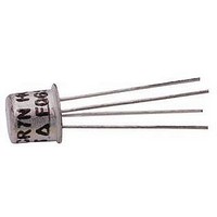
MOSFET Small Signal 40V 5mA 375mW

3N163-E3

Manufacturer Part Number
3N163-E3
Description
MOSFET Small Signal 40V 5mA 375mW
Manufacturer
Vishay
Datasheets

Specifications of 3N163-E3

Transistor Polarity
P-Channel
Minimum Operating Temperature
- 55 C
Configuration
Single
Resistance Drain-source Rds (on)
250 Ohm @ 20 V
Drain-source Breakdown Voltage
40 V
Gate-source Breakdown Voltage
+/- 30 V
Continuous Drain Current
0.05 A
Power Dissipation
375 mW
Maximum Operating Temperature
+ 150 C
Mounting Style
SMD/SMT
Package / Case
TO-206AF
Continuous Drain Current Id
-50mA
Drain Source Voltage Vds
-40V
On Resistance Rds(on)
250ohm
Rds(on) Test Voltage Vgs
-20V
Threshold Voltage Vgs Typ
-2.5V
Lead Free Status / RoHS Status
Lead free / RoHS Compliant
Lead Free Status / RoHS Status
Lead free / RoHS Compliant, Lead free / RoHS Compliant
Product Summary
Description
The 3N163/164 are lateral p-channel MOSFETs designed
for analog switch and preamplifier applications where
high speed and low parasitic capacitances are required.
Absolute Maximum Ratings (T
Continuous Drain Current
Lead Temperature (
Updates to this data sheet may be obtained via facsimile by calling Siliconix FaxBack, 1-408-970-5600. Please request FaxBack document #70228.
P-Channel Enhancement-Mode MOSFET Transistors
Siliconix
P-37404—Rev. D, 04-Jul-94
Features
Number
3N163
3N164
Ultra-Low Input Leakage: 0.02 pA Typ.
High Gate Breakdown Voltage:
Normally Off
Part
V
(BR)DSS
1
/
16
” from case for 10 seconds)
(V)
–40
–30
. . . . . . . . . . . . . . . . . . . . . . . . . . . .
Min
V
–2 to –5
–2 to –5
GS(th)
(V)
125 V
. . . . . . . . .
Benefits
r
High Input Impedance Isolation
Minimize Handling ESD Problems
High Off Isolation without Power
DS(on)
G
D
( )
250
300
–50 mA
300 C
–40
Max
1
2
A
TO-206AF
Top View
(TO-72)
= 25 C Unless Otherwise Noted)
The hermetic TO-206AF package is compatible with
military processing per military standards (see Military
information).
Storage Temperature
Operating Junction Temperature
Power Dissipation
Notes:
a.
I
D(on)
(mA)
Derate 3 mW/ C above 25 C
4
3
–5
–3
Min
S
Substrate
Case
C
a
rss
. . . . . . . . . . . . . . . . . . . . . . . . . . . . . . . . .
(pF)
0.7
0.7
. . . . . . . . . . . . . . . . . . . . . . . . . . .
Applications
Max
Ultra-High Input Impedance Amplifier
Smoke Detectors
Electrometers
Analog Switching
Digital Switching
3N163/3N164
. . . . . . . . . . . . . . . . . .
t
ON
(ns)
18
18
Typ
–65 to 200 C
–55 to 150 C
375 mW
1

Related parts for 3N163-E3

3N163-E3 Summary of contents

Page 1

... Ultra-Low Input Leakage: 0.02 pA Typ. High Gate Breakdown Voltage: 125 V Normally Off Description The 3N163/164 are lateral p-channel MOSFETs designed for analog switch and preamplifier applications where high speed and low parasitic capacitances are required. Absolute Maximum Ratings (T Continuous Drain Current ...

Page 2

... V = – – oss MHz rss – 1500 = 1500 –10 mA – GEN 3N163 3N164 –70 –40 –30 –70 –40 – –2.5 –2 –5 –2 –5 –3.5 –3 –6.5 –2.5 –6.5 <–1 –10 –1 <–1 –10 pA –1 –8 –200 –400 –20 nA –10 –400 – ...

Page 3

... V = – kHz – –4 V 100 = –0.4 –0.01 Low-Level Drain-Source On-Voltage 2.5 = 100 2.0 1.5 1.0 0.5 0 –20 0 3N163/3N164 Transfer Characteristics GS –8 –12 –16 –20 V – Gate-Source Voltage (V) GS vs. Drain Current 125 C –0.1 –1 –10 I – Drain Current (mA) D vs. Gate-Source Voltage –10 – ...

Page 4

... Typical Characteristics (Cont’d) Capacitance vs. Gate-Source Voltage 3.0 C iss 2 oss DS 1 MHz 1.2 0 –4 –8 –12 V – Gate-Source Voltage (V) GS Common-Source Output Conductance vs. Drain Voltage kHz –10 mA D(on) 100 – –5 –10 –15 –20 V – Drain-Source Voltage (V) DS Switching Time Test Circuit To Scope – ...

Page 5

... Vishay disclaims any and all liability arising out of the use or application of any product described herein or of any information provided herein to the maximum extent permitted by law. The product specifications do not expand or otherwise modify Vishay’ ...

Related keywords