MAX98088EWY+T Maxim Integrated Products, MAX98088EWY+T Datasheet - Page 120
MAX98088EWY+T
Manufacturer Part Number
MAX98088EWY+T
Description
Audio CODECs DUAL I2S CODEC AUDIO STEREO
Manufacturer
Maxim Integrated Products
Datasheet
1.MAX98088EWYT.pdf
(123 pages)
Specifications of MAX98088EWY+T
Number Of Adc Inputs
2
Number Of Dac Outputs
2
Resolution
24 bit
Operating Supply Voltage
1.8 V
Maximum Operating Temperature
+ 85 C
Mounting Style
SMD/SMT
Package / Case
WLP-63
Number Of Channels
2
Supply Current
4.5 mA
Thd Plus Noise
- 77 dB
Lead Free Status / RoHS Status
Lead free / RoHS Compliant


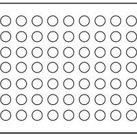
The IC uses a 63-bump WLP package. Figure 42
provides an example of how to connect to all active
bumps using 3 layers of the PCB. To ensure uninter-
rupted ground returns, use layer 2 as a connecting layer
between layer 1 and layer 2 and flood the remaining area
with ground.
Stereo Audio Codec
with FlexSound Technology
120
Figure 42. Suggested Routing for the MAX98088
Recommended PCB Routing
LAYER 2
LAYER 3
LAYER 1
Proper layout and grounding are essential for optimum
performance. When designing a PCB for the ICs, parti-
tion the circuitry so that the analog sections of the IC are
separated from the digital sections. This ensures that the
analog audio traces are not routed near digital traces.
Use a large continuous ground plane on a dedicated
layer of the PCB to minimize loop areas. Connect AGND,
DGND, HPGND, SPKLGND, and SPKRGND directly to
the ground plane using the shortest trace length pos-
sible. Proper grounding improves audio performance,
minimizes crosstalk between channels, and prevents any
digital noise from coupling into the analog audio signals.
Ground the bypass capacitors on MICBIAS, REG, PREG,
and REF directly to the ground plane with minimum
trace length. Also be sure to minimize the path length to
AGND. Bypass AVDD directly to AGND.
Connect all digital I/O termination to the ground plane
with minimum path length to DGND. Bypass DVDD,
DVDDS1, and DVDDS2 directly to DGND.
Place the capacitor between C1P and C1N as close as
possible to the ICs to minimize trace length from C1P to
C1N. Inductance and resistance added between C1P
and C1N reduce the output power of the headphone
amplifier. Bypass HPVSS with a capacitor located close
to HPVSS with a short trace length to HPGND. Close
decoupling of HPVSS minimizes supply ripple and maxi-
mizes output power from the headphone amplifier.
HPSNS senses ground noise on the headphone jack and
adds the same noise to the output audio signal, thereby
making the output (headphone output minus ground)
noise free. Connect HPSNS to the headphone jack shield
to ensure accurate pickup of headphone ground noise.
Bypass SPKLVDD and SPKRVDD to SPKLGND and
SPKRGND, respectively, with as little trace length as
possible. Connect SPKLP, SPKLN, SPKRP, and SPKRN
to the stereo speakers using the shortest traces pos-
sible. Reducing trace length minimizes radiated EMI.
Route SPKLP/SPKLN and SPKRP/SPKRN as differential
pairs on the PCB to minimize loop area, thereby the
inductance of the circuit. If filter components are used
on the speaker outputs, be sure to locate them as close
as possible to the IC to ensure maximum effectiveness.
Minimize the trace length from any ground-connected
passive components to SPKLGND and SPKRGND to
further minimize radiated EMI.
Supply Bypassing, Layout, and Grounding
Related parts for MAX98088EWY+T
Image
Part Number
Description
Manufacturer
Datasheet
Request
R

Part Number:
Description:
Stereo Audio Codec With Flexsound Technology
Manufacturer:
Maxim Integrated Products, Inc.
Datasheet:

Part Number:
Description:
MAX7528KCWPMaxim Integrated Products [CMOS Dual 8-Bit Buffered Multiplying DACs]
Manufacturer:
Maxim Integrated Products
Datasheet:
Part Number:
Description:
Single +5V, fully integrated, 1.25Gbps laser diode driver.
Manufacturer:
Maxim Integrated Products
Datasheet:
Part Number:
Description:
Single +5V, fully integrated, 155Mbps laser diode driver.
Manufacturer:
Maxim Integrated Products
Datasheet:
Part Number:
Description:
VRD11/VRD10, K8 Rev F 2/3/4-Phase PWM Controllers with Integrated Dual MOSFET Drivers
Manufacturer:
Maxim Integrated Products
Datasheet:
Part Number:
Description:
Highly Integrated Level 2 SMBus Battery Chargers
Manufacturer:
Maxim Integrated Products
Datasheet:
Part Number:
Description:
Current Monitor and Accumulator with Integrated Sense Resistor; ; Temperature Range: -40°C to +85°C
Manufacturer:
Maxim Integrated Products
Part Number:
Description:
TSSOP 14/A�/RS-485 Transceivers with Integrated 100O/120O Termination Resis
Manufacturer:
Maxim Integrated Products
Part Number:
Description:
TSSOP 14/A�/RS-485 Transceivers with Integrated 100O/120O Termination Resis
Manufacturer:
Maxim Integrated Products
Part Number:
Description:
QFN 16/A�/AC-DC and DC-DC Peak-Current-Mode Converters with Integrated Step
Manufacturer:
Maxim Integrated Products
Part Number:
Description:
TDFN/A/65V, 1A, 600KHZ, SYNCHRONOUS STEP-DOWN REGULATOR WITH INTEGRATED SWI
Manufacturer:
Maxim Integrated Products
Part Number:
Description:
Integrated Temperature Controller f
Manufacturer:
Maxim Integrated Products
Part Number:
Description:
SOT23-6/I�/45MHz to 650MHz, Integrated IF VCOs with Differential Output
Manufacturer:
Maxim Integrated Products
Part Number:
Description:
SOT23-6/I�/45MHz to 650MHz, Integrated IF VCOs with Differential Output
Manufacturer:
Maxim Integrated Products
Part Number:
Description:
EVALUATION KIT/2.4GHZ TO 2.5GHZ 802.11G/B RF TRANSCEIVER WITH INTEGRATED PA
Manufacturer:
Maxim Integrated Products