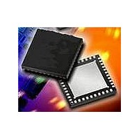
MAX2067ETL+ Maxim Integrated Products, MAX2067ETL+ Datasheet - Page 18

MAX2067ETL+
Manufacturer Part Number
MAX2067ETL+
Description
RF Amplifier IC VGA PROG ANALG-EP h-Linearity, Serial-
Manufacturer
Maxim Integrated Products
Datasheet
1.MAX2067EVKIT.pdf
(23 pages)
Specifications of MAX2067ETL+
Bandwidth
1000 MHz
Mounting Style
SMD/SMT
Operating Supply Voltage
5 V
Supply Current
72 mA
Maximum Power Dissipation
6.5 W
Maximum Operating Temperature
+ 85 C
Minimum Operating Temperature
- 40 C
Package / Case
TQFN-40
Lead Free Status / RoHS Status
Lead free / RoHS Compliant
50MHz to 1000MHz High-Linearity,
Serial/Analog-Controlled VGA
The MAX2067 high-linearity analog variable-gain ampli-
fier is a general-purpose, high-performance amplifier
designed to interface with 50Ω systems operating in the
50MHz to 1000MHz frequency range.
The MAX2067 integrates an analog attenuator to provide
31dB of total gain control, as well as a driver amplifier
optimized to provide high gain, high IP3, low noise figure,
and low power consumption. For applications that do not
require high linearity, the bias current of the amplifier can
be adjusted by an external resistor to further reduce
power consumption.
The analog attenuator is controlled using an external
voltage or through the SPI-compatible interface using
an on-chip DAC. Because each stage has its own exter-
nal RF input and RF output, this component can be con-
figured to either optimize NF (amplifier configured first),
or OIP3 (amplifier last). The device’s performance fea-
tures include 22dB stand-alone amplifier gain (amplifier
only), 4dB NF at maximum gain (includes attenuator
insertion loss), and a high OIP3 level of +43dBm. Each
of these features makes the MAX2067 an ideal VGA for
numerous receiver and transmitter applications.
In addition, the MAX2067 operates from a single +5V
supply, or a single +3.3V supply with slightly reduced
performance, and has adjustable bias to trade current
consumption for linearity performance.
The MAX2067’s analog attenuator has a dynamic range
of 31dB and is controlled using an external voltage or
through the 3-wire SPI using an on-chip 8-bit DAC. See
the Applications Information section and Table 1 for
attenuator programming details. The attenuator can be
used for both static and dynamic power control.
Table 1. Control Logic
X = Don’t care.
MICROWIRE is a trademark of National Semiconductor Corp.
18
VDAC_EN
______________________________________________________________________________________
0
1
1
VR EF _ SEL EC T
Detailed Description
X
1
0
Analog Attenuator
Controlled by external control voltage
Controlled by on-chip DAC
Controlled by on-chip DAC
ANALOG ATTENUATOR
The MAX2067 includes a high-performance driver with
a fixed gain of 22dB. The driver amplifier circuit is opti-
mized for high linearity for the 50MHz to 1000MHz fre-
quency range.
The analog attenuator is controlled by either an external
control voltage applied at ANALOG_VCTRL (pin 39) or
by the on-chip 8-bit DAC. Through the utilization of this
control DAC, the user can easily adjust the analog
attenuation in 0.12dB increments through a simple SPI
command. The DAC enable/disable logic-input pin
(VDAC_EN), and the DAC reference voltage selection
logic-input pin (VREF_SELECT) determine how the
attenuator is controlled. When the DAC is enabled,
either the on-chip voltage reference or the external volt-
age reference can be selected. See Table 1 for the
attenuator and DAC operation truth table.
Although this on-chip DAC eliminates the need for an
external analog control voltage, the user still has the
option of disabling the DAC and using an external ana-
log control voltage for instances where additional atten-
uation resolution is needed, or in cases where the gain
trim/automatic gain-control (AGC) loop is purely analog.
The MAX2067 employs a 3-wire SPI/MICROWIRE™-
compatible serial interface to program the on-chip DAC.
Eight bits of data are shifted in MSB first and framed by
CS. When CS is low, the clock is active and data is
shifted on the rising edge of the clock. When CS transi-
tions high, the data is latched and the attenuator setting
changes (Figure 1). See Table 2 for details on the SPI
data format.
SPI Interface and Attenuator Settings
Disabled
Enabled (DAC uses on-chip voltage reference)
E nab l ed ( D AC uses exter nal vol tag e r efer ence)
Applications Information
D/A CONVERTER
Attenuator Control
Driver Amplifier


