TQP3M9009-PCB-RF TriQuint, TQP3M9009-PCB-RF Datasheet - Page 8
TQP3M9009-PCB-RF
Manufacturer Part Number
TQP3M9009-PCB-RF
Description
RF Amplifier Eval Bd .5-4GHz
Manufacturer
TriQuint
Type
High Linearity Amplifierr
Datasheet
1.TQP3M9009-PCB-RF.pdf
(10 pages)
Specifications of TQP3M9009-PCB-RF
Bandwidth
1.9 GHz
Mounting Style
SMD/SMT
Number Of Channels
1
Operating Frequency
500 MHz to 4000 MHz
P1db
21.9 dBm
Noise Figure
1.3 dB
Operating Supply Voltage
4.75 V to 5.25 V
Supply Current
125 mA
Maximum Operating Temperature
+ 85 C
Minimum Operating Temperature
- 40 C
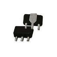
Package / Case
SOT-89
Lead Free Status / RoHS Status
Lead free / RoHS Compliant
Other names
1073467


TQP3M9009
Advanced Data Sheet: Rev B 03/29/10
© 2009 TriQuint Semiconductor, Inc.
High Linearity LNA Gain Block
Pin Configuration and Description
Applications Information
PC Board Layout
Top RF layer is .014” NELCO N4000-13, є
layers (0.062” thick) for mechanical rigidity.
layers are 1-oz copper. 50 ohm Microstrip line details:
width = .029”, spacing = .035”.
The pad pattern shown has been developed and tested for
optimized assembly at TriQuint Semiconductor.
PCB land pattern has been developed to accommodate
lead and package tolerances.
processes vary from supplier to supplier, careful process
development is recommended.
Pin
1
2, 4
3
Symbol
RF IN
GND
RFout / Vdd
Since surface mount
Description
Input, matched to 50 ohms, External DC block is required.
Needed for RF and the thermal path
Output, matched to 50 ohms, External DC Block is required and supply voltage
r
= 3.9, 4 total
Metal
RF IN
The
1
- 8 of 10 -
GND
GND
2
4
RF OUT
3
Connecting the Digital World to the Global Network
Disclaimer: Subject to change without
noticee
®
Related parts for TQP3M9009-PCB-RF
Image
Part Number
Description
Manufacturer
Datasheet
Request
R

Part Number:
Description:
RF Amplifier Eval Bd .05-.5GHz
Manufacturer:
TriQuint
Datasheet:

Part Number:
Description:
RF Amplifier 50MHz to 4000MHz 5Volts 21.8dB Gain
Manufacturer:
TriQuint
Datasheet:

Part Number:
Description:
Manufacturer:
TriQuint
Datasheet: