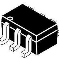
MBC13720-1900EVK Freescale Semiconductor, MBC13720-1900EVK Datasheet - Page 16

MBC13720-1900EVK
Manufacturer Part Number
MBC13720-1900EVK
Description
RF Modules & Development Tools LNA W/BYPASS SWITCH
Manufacturer
Freescale Semiconductor
Datasheet
1.MBC13720-900EVK.pdf
(24 pages)
Specifications of MBC13720-1900EVK
Board Size
2.2 mm x 2.2 mm x 1.1 mm
Product
RF Modules
Maximum Frequency
1900 MHz
Supply Voltage (max)
3.3 V
Lead Free Status / Rohs Status
Lead free / RoHS Compliant
Application Information
5
The MBC13720 SiGe:C LNA is designed for applications in the 400 MHz to 2.4 GHz range. It has four
different modes: Low IP3, High IP3, Bypass, and Standby. The IC is programmable through the Enable 1
and Enable 2 pins. In Low IP3 mode, current consumption is optimized. Current consumption is higher in
High IP3 mode to boost the intercept point performance. The gain difference between Low IP3 and High
IP3 modes is typically 1.0 dB; and typically the Low IP3 mode has a slightly better noise figure
performance.
The internal bypass switch is designed for broadband applications. One of the advantages of the
MBC13720 is the simplification of the matching network in both bypass and amplifier modes. The bypass
switch is designed so that changes of input and output return losses between bypass mode and amplifier
mode are minimized. As a result, the mismatch at the LNA input and output is minimized and the matching
network design is simplified.
In the design of the external matching network, conjugate matching does not necessarily provide the best
noise figure performance. Balancing between noise figure, gain, and intercept point is the major design
consideration. Typical circuits are provided in
applications.
Figure 2
gain, and return losses are optimized. L1 and C2 act as a low frequency trap to improve the input intercept
point.
In
used to maximize the input intercept point. It has moderate IP3 performance and high gain.
the 900 MHz application circuit with feedback network for higher IP3. Capacitive feedback is used to
increase the 3rd order input intercept point while decreasing gain and provides unconditional stability.
The corresponding PCBs are shown in
the 1900 MHz, 900 MHz, and High IP3 900 MHz application circuits. Typical characteristics of the
application boards are shown in
16
Figure
Application Information
shows the typical application circuit at 1.9 and 2.4 GHz. The noise figure, input intercept point,
3, the typical application circuit for 900 MHz is shown. The input low frequency trap again is
. 33pf
C 7
8. 2 nH
Enable1
27 pf
0.1 uf
C 1
C 2
L 1
Figure 6. Typical 1.9 and 2.4 GHz LNA Application Schematic
Table
4
5
6
MBC13720 Technical Data, Rev. 3.5
17.
Figure 9
Control
Bias
Figure 2
through
and
Figure
Figure 3
3
2
1
11.
330 Ω
Table 16
R1
for 1.9 GHz, 2.4 GHz and 900 MHz
1. 0 pf
Enable2
C 3
lists the bill of materials for
Vcc
27 pF
C4
33 pf
C 5
2. 7 nH
L2
Freescale Semiconductor
OUT
RF
0.1 uf
C6
Figure 4
shows


