ZEN132V075A48LS-TB Tyco Electronics, ZEN132V075A48LS-TB Datasheet - Page 3
ZEN132V075A48LS-TB
Manufacturer Part Number
ZEN132V075A48LS-TB
Description
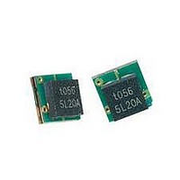
Power Management Modules & Development Tools PolyZen Micro-Assem on Test Board
Manufacturer
Tyco Electronics
Type
Power Factor Correctionr
Datasheet
1.ZEN056V130A24LS-TB.pdf
(8 pages)
Specifications of ZEN132V075A48LS-TB
Input Voltage
13.4 V
Maximum Operating Temperature
+ 85 C
Minimum Operating Temperature
- 40 C
Operating Supply Voltage
48 V
Product
Power Management Modules
For Use With/related Products
ZEN132V075A48LS
Lead Free Status / RoHS Status
Lead free / RoHS Compliant


5.45
Min
308 Constitution Drive
Menlo Park, CA 94025-1164
Phone: 800-227-4856
www.circuitprotection.com
GENERAL SPECIFICATIONS
ELECTRICAL CHARACTERISTICS
Note 1: Electrical characteristics determined at 25ºC unless otherwise specified.
Note 2:
Note 3:
Note 4:
Note 5:
Note 6:
Note 7:
Note 8:
Note 9:
Note 10: The power dissipated by the device when in the “tripped” state, as measured on TE test boards (see note 3).
Note 11: Specifications based on limited qualification data and subject to change.
MECHANICAL DIMENSIONS
Typ
V
(V)
5.6
Z
4
This device is intended for limited fault protection. Repeated trip events or extended trip endurance can degrade the device
and may affect performance to specifications. Performance impact will depend on multiple factors including, but not limited to,
voltage, trip current, trip duration, trip cycles, and circuit design. For details or ratings specific to your application contact Tyco
Electronics Circuit Protection directly.
Specifications developed using 1.0 ounce 0.045” wide copper traces on dedicated FR4 test boards. Performance in your
application may vary.
I
I
specified temperature. Specification assumes I
the diode from acting as a heat source. Testing is conducted with an “open” Zener.
R Typ: Resistance between V
R
soldering.
V
the voltage (V
and 24hours trip endurance at the specified voltage (V
"shorted" load (V
I
condition, prior to a trip event. I
lots) survived 100 test cycles. RMS fault currents above I
device. Testing is conducted with NO load connected to V
between V
the diode. I
zt
HOLD
FLT
INT
1Max
is the current at which V
Max: I
5.75
Max
Max: V
: Maximum steady state I
: The maximum resistance between V
FLT
IN
0.1
(A)
I
FLT
INT
zt
4
to GND and includes the PolyZen Diode drop. Specification is dependent on the direction of current flow through
Max relates to the stead state current flowing through the diode portion of the PolyZen device in a fault
Max is a survivability rating, not a performance rating.
Max relates to the voltage across the PPTC portion of the PolyZen device (V
IN
-V
OUT
@
I
HOLD
20ºC
OUT
(A)
1.3
= 0V). V
) at which typical qualification devices (98% devices, 95% confidence) survived at least 100 trip cycles
5
z
Voltage
Leakage Current
is measured (V
Raychem Circuit Protection Products
Test
5.25
INT
IN
PTC
FLT
Polymer Enhanced Zener Diode
and V
Max is a survivability rating, not a performance rating.
Operating Temperature
Storage Temperature
(current entering or exiting the V
Max is defined as the current at which typical qualification devices (12 parts per lot from 3
Current
OUT
(mA)
1-3, 11
Max
10
Micro-Assemblies
pins during normal operation at room temperature.
Z
IN
PolyZen
= V
and V
(Typical unless otherwise specified)
FLT
(Ohms)
R Typ
OUT
0.12
(current flowing through the Zener diode) is sufficiently low so as to prevent
OUT
). Additional V
Length
Height
Diode
Diode
Length
Height
Width
Offset
Offset
6
IN
pins at room temperature, one hour after 1
-V
FLT
OUT
OUT
(Ohms)
R
0.16
Max may permanently damage the diode portion of the PolyZen
1Max
, such that I
) and current (I
7
Hd
O1
O2
Ld
-40º to +85ºC
-40º to +85ºC
Z
W
H
L
IN
values are available on request.
pin of the device) that will not generate a trip event at the
Max
24V
V
(V)
INT
OUT
V
3.85 mm
3.85 mm
Int
(0.152”)
(0.152”)
(0.055”)
1.4mm
(V)
PTC
= 0. “Test voltage” is defined as the voltage
Max
Min
Current
-
-
-
-
). V
Test
(A)
8
3A
INT
PRODUCT: ZEN056V130A24LS
DOCUMENT: SCD 26730
REV LETTER: E
REV DATE: OCTOBER 27, 2008
PAGE NO.: 3 OF 8
Max testing is conducted using a
(0.067”)
(0.118”)
(0.039”)
(0.024”)
(0.028”)
1.7 mm
3.0 mm
1.0 mm
0.6 mm
0.7 mm
Typical
I
(0.16”)
(0.16”)
FLT
4 mm
4 mm
IN
+10
(A)
-40
Max
-V
I
FLT
OUT
Max
st
). V
Voltage
trip or after reflow
9
Test
-16V
4.15 mm
4.15 mm
+24
INT
(0.163")
(0.163")
(0.081”)
(V)
2.0 mm
Max
Max is defined as
-
-
-
-
Value
(W)
1.0
Tripped Power
Dissipation
Max
Voltage
Test
(V)
24
10
Related parts for ZEN132V075A48LS-TB
Image
Part Number
Description
Manufacturer
Datasheet
Request
R

Part Number:
Description:
Battery Interconnection System for Portable Electronics; BU CONN FS6 8POS DIP TYPE ASSY ( AMP )
Manufacturer:
Tyco Electronics
Part Number:
Description:
Manufacturer:
Tyco Electronics
Datasheet:
Part Number:
Description:
Manufacturer:
Tyco Electronics
Datasheet:


