NV8664ST50T3GEVB ON Semiconductor, NV8664ST50T3GEVB Datasheet
NV8664ST50T3GEVB
Specifications of NV8664ST50T3GEVB


Related parts for NV8664ST50T3GEVB

NV8664ST50T3GEVB Summary of contents
Page 1
NCV8664 Very Low I Low Dropout q Linear Regulator The NCV8664 is a precision 3.3 V and 5.0 V fixed output, low dropout integrated voltage regulator with an output current capability of 150 mA. Careful management of light load current ...
Page 2
IN Bias Current Generators 1.3 V Reference PIN FUNCTION DESCRIPTION Pin No. DPAK/SOT−223 SOIC−8 Symbol GND TAB − GND − 1, 5−8 NC OPERATING RANGE Pin Symbol, Parameter , V DC Input ...
Page 3
LEAD SOLDERING TEMPERATURE AND MSL Rating Lead Temperature Soldering Reflow (SMD Styles Only), Lead Free (Note 3) Moisture Sensitivity Level 3. Lead Free, 60 sec – 150 sec above 217°C, 40 sec max at peak. ELECTRICAL CHARACTERISTICS Characteristic Output Voltage ...
Page 4
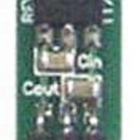
I 4.5− Input C IN 100 nF 1.0 mF Figure 2. Measurement Circuit 4.5− Input C IN 100 nF Figure 3. Applications Circuit http://onsemi.com I Output V Q out 8664 ...
Page 5
Stable Region 0. 100 LOAD CURRENT (mA) Figure 4. ESR Characterization, 5.0 V Version 9 7.0 6.0 5.0 4.0 3.0 2.0 1 ...
Page 6
OUTPUT LOAD (mA) Figure 10. Dropout Voltage vs. Output Load, 5.0 V Version 160 140 120 100 125° ...
Page 7
OUTPUT LOAD (mA) Figure 15. ESR Stability, 3.3 V Version 9.0 8.0 7.0 6.0 5.0 4.0 3.0 2.0 1 100 OUTPUT ...
Page 8
OUTPUT LOAD (mA) Figure 21. Dropout Voltage, 3.3 V Version 3.50 3.45 3.40 3.35 3.30 3.25 3.20 3.15 3.10 3.05 3.00 −40 − ...
Page 9
... These values appear in data sheets ≥ and OUT of heat sink manufacturers. Thermal, mounting, and heat ≥ and ESR sinking are discussed in the ON Semiconductor application note AN1040/D, available on the ON Semiconductor Website. http://onsemi.com 9 I Q(max I(max the quiescent current the regulator q ...
Page 10
EMC−Characteristics: Conducted Susceptibility All EMC−Characteristics are based on limited samples and not part of production testing, according to 47A/658/CD IEC62132−4 (Direct Power Injection) Test Conditions Supply Voltage Temperature T = 23°C ±5°C A Load R ...
Page 11
ORDERING INFORMATION Device NCV8664D50R2G NCV8664D50G NCV8664DT50RKG NCV8664DT33RKG NCV8664ST50T3G NCV8664ST33T3G †For information on tape and reel specifications, including part orientation and ...
Page 12
... A 0.08 (0003) A1 2.0 0.079 *For additional information on our Pb−Free strategy and soldering details, please download the ON Semiconductor Soldering and Mounting Techniques Reference Manual, SOLDERRM/D. PACKAGE DIMENSIONS SOT−223 (TO−261) CASE 318E−04 ISSUE M NOTES: 1. DIMENSIONING AND TOLERANCING PER ANSI Y14.5M, 1982. ...
Page 13
... DETAIL 0.005 (0.13 *For additional information on our Pb−Free strategy and soldering details, please download the ON Semiconductor Soldering and Mounting Techniques Reference Manual, SOLDERRM/D. PACKAGE DIMENSIONS DPAK (SINGLE GAUGE) DT SUFFIX CASE 369C−01 ISSUE GAUGE L2 SEATING C PLANE PLANE DETAIL A ROTATED SOLDERING FOOTPRINT* 6 ...
Page 14
... *For additional information on our Pb−Free strategy and soldering details, please download the ON Semiconductor Soldering and Mounting Techniques Reference Manual, SOLDERRM/D. ON Semiconductor and are registered trademarks of Semiconductor Components Industries, LLC (SCILLC). SCILLC reserves the right to make changes without further notice to any products herein. SCILLC makes no warranty, representation or guarantee regarding the suitability of its products for any particular purpose, nor does SCILLC assume any liability arising out of the application or use of any product or circuit, and specifically disclaims any and all liability, including without limitation special, consequential or incidental damages. “ ...