UM232R FTDI, UM232R Datasheet - Page 7
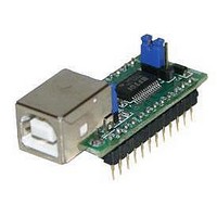
UM232R
Manufacturer Part Number
UM232R
Description
Interface Modules & Development Tools USB to Serial UART Dev Mod for FT232R
Manufacturer
FTDI
Type
Development Moduler
Specifications of UM232R
Interface Type
USB, Serial, UART
Data Bus Width
Serial
Operating Supply Voltage
1.8 V to 5.25 V
Product
Interface Modules
Supported Devices
FT232R
Svhc
No SVHC (18-Jun-2010)
Development Tool Type
Development Kit
Kit Features
Single Chip USB To Asynchronous Serial Data Transfer Interface, Auto Transmit Buffer
Rohs Compliant
Yes
Supported Families
FT232RL
Features
Single Chip USB To Asynchronous Serial Data Transfer Interface, Auto Transmit Buffer Control
Tool / Board Applications
USB To
For Use With/related Products
FT232R
Lead Free Status / RoHS Status
Lead free / RoHS Compliant


Table 1 - Module Pin Out Description
* When used in Input Mode, these pins are pulled to VCCIO via internal 200kΩ resistors. These pins can be
programmed to gently pull low during USB suspend ( PWREN# = “1” ) by setting an option in the internal EEPROM.
UM232R USB-Serial UART Development Module Datasheet Version 1.02
Pin No. Name
1
2
3
4
5
6
7, 24
8
9
10
11
12
13
14
15, 21
16
17
19
20
18
22
23
3.2 Signal Descriptions
TXD
DTR#
RTS#
VIO
RXD
RI#
GND
DSR#
DCD#
CTS#
CB4
CB2
SLD
USB
VCC
PU2
PU1
3V3
RST#
CB3
CB1
CB0
Type
Output
Output
Output
PWR
Input
Input
PWR
Input
Input
Input
I/O
I/O
GND
Output
PWR
or
Output
Control
Control
Output
Input
I/O
I/O
I/O
Description
Transmit Asynchronous Data Output.*
Data Terminal Ready Control Output / Handshake signal.*
Request To Send Control Output / Handshake signal.*
+1.8V to +5.25V supply to the UART Interface and CBUS I/O pins (1...3, 5, 6, 9...14, 22, 23).
In USB bus powered designs connect to 3V3 to drive out at 3.3V levels (connect jumper J1 pins 1 and 2
together), or connect to VCC to drive out at 5V CMOS level (connect jumper J1 pins 2 and 3 together). This
pin can also be supplied with an external 1.8V - 2.8V supply in order to drive out at lower levels. It should be
noted that in this case this supply should originate from the same source as the supply to Vcc. This means
that in bus powered designs a regulator which is supplied by the 5V on the USB bus should be used.
Receive Asynchronous Data Input.*
Ring Indicator Control Input. When remote wake up is enabled in the internal EEPROM taking RI# low can be
used to resume the PC USB host controller from suspend.*
Module ground supply pins
Data Set Ready Control Input / Handshake signal.*
Data Carrier Detect Control input.*
Clear to Send Control input / Handshake signal.*
Configurable CBUS I/O Pin. Function of this pin is configured in the device internal EEPROM. Factory Default
pin function is SLEEP#. See CBUS Signal Options,
Configurable CBUS I/O Pin. Function of this pin is configured in the device internal EEPROM. Factory Default
pin function is TXDEN. See CBUS Signal Options,
USB Cable shield.
5V Power output USB port. For a low power USB bus powered design, up to 100mA can be sourced from the
5V supply on the USB bus. A maximum of 500mA can be sourced from the USB bus in a high power USB bus
powered design.
These two pins are internally connected on the module pcb. To power the module from the 5V supply on USB
bus connect jumper J2 pins 1 and 2 together (this is the module default configuration). In this case these pins
would have the same description as pin 14.
To use the UM232R module in a self powered configuration ensure that jumper J2 pins 1 and 2 are not con-
nected together, and apply an external 3.3V to 5.25V supply to one of these pins.
Pull up resistor pin connection 2. Conect to pin 17 (RST#) in a self powered configuration.
Pull up resistor pin connection 1. Connect to pin 14 (USB) in a self powered configuration
3.3V output from integrated L.D.O. regulator. This pin is decoupled to ground on the module pcb with a 10nF
capacitor. The prime purpose of this pin is to provide the internal 3.3V supply to the USB transceiver cell and
the internal 1.5kΩ pull up resistor on USBDP. Up to 50mA can be drawn from this pin to power external logic if
required. This pin can also be used to supply the FT232RL’s VCCIO pin by connecting this pin to pin 4 (VIO),
or by connecting together pins 1 and 2 on jumper J1.
Can be used by an external device to reset the FT232R. If not required can be left unconnected, or pulled up
to VCCIO.
Configurable CBUS I/O Pin. Function of this pin is configured in the device internal EEPROM. Factory Default
pin function is PWREN#. See CBUS Signal Options,
Configurable CBUS I/O Pin. Function of this pin is configured in the device internal EEPROM. Factory Default
pin function is RXLED#. See CBUS Signal Options,
Configurable CBUS I/O Pin. Function of this pin is configured in the device internal EEPROM. Factory Default
pin function is TXLED#. See CBUS Signal Options,
Table
Table
Table
Table
Table
© Future Technology Devices International Ltd. 2005
4.*
4.*
4.*
4.*
4.*
Related parts for UM232R
Image
Part Number
Description
Manufacturer
Datasheet
Request
R

Part Number:
Description:
Interface Modules & Development Tools USB to Serial UART MiniB Dev Mod FT232R
Manufacturer:
FTDI
Datasheet:

Part Number:
Description:
BOARD, EVALUATION, EU PSU
Manufacturer:
FTDI
Datasheet:
Part Number:
Description:
BOARD, EVALUATION, UK PSU
Manufacturer:
FTDI
Datasheet:
Part Number:
Description:
BOARD, EVALUATION, US PSU
Manufacturer:
FTDI
Datasheet:
Part Number:
Description:
Specifications: Manufacturer: FTDI ; Product Category: USB Interface IC ; RoHS: Details ; Operating Supply Voltage: 3 V to 5.25 V ; Supply Current: 25 mA ; Maximum Operating Temperature: + 70 C ; Mounting Style: SMD/SMT ; Package / Case: QFN-32
Manufacturer:
FTDI
Part Number:
Description:
integr. usb2.0/uart lqfp32 rohs ftdi reel c1k...
Manufacturer:
FTDI
Datasheet:
Part Number:
Description:
Interface Development Tools USB to UART Breakout Board
Manufacturer:
FTDI
Datasheet:

Part Number:
Description:
IC USB TO SERIAL UART 32-QFN
Manufacturer:
FTDI, Future Technology Devices International Ltd

Part Number:
Description:
USB Interface IC USB to Serial UART Enhanced IC SSOP-28
Manufacturer:
FTDI
Datasheet:

Part Number:
Description:
IC, USB UART INTERFACE, SSOP-28
Manufacturer:
FTDI
Datasheet:

Part Number:
Description:
IC, USB UART INTERFACE, QFN-32
Manufacturer:
FTDI
Datasheet:
Part Number:
Description:
IC, USB FIFO INTERFACE, SSOP-28
Manufacturer:
FTDI
Datasheet:
Part Number:
Description:
MODULE, USB, 4 PORT, FT4232H BASED
Manufacturer:
FTDI
Datasheet:
Part Number:
Description:
357-036-542-201 CARDEDGE 36POS DL .156 BLK LOPRO
Manufacturer:
FTDI
Datasheet:
Part Number:
Description:
357-036-542-201 CARDEDGE 36POS DL .156 BLK LOPRO
Manufacturer:
FTDI
Datasheet: