VNCLO-SHLD-1A FTDI, VNCLO-SHLD-1A Datasheet - Page 13
VNCLO-SHLD-1A
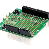
Manufacturer Part Number
VNCLO-SHLD-1A
Description
Interface Modules & Development Tools Vinculo Prototyping Shield Accessory
Manufacturer
FTDI
Datasheet
1.VNCLO-MB1A.pdf
(26 pages)
Specifications of VNCLO-SHLD-1A
Interface Type
USB, Serial, UART, FIFO, SPI
Data Bus Width
Serial, 8 bit
Operating Supply Voltage
100 VAC to 240 VAC
Product
Interface Development Tools
Features
Precompiled Drivers For A Variety Of Interfaces
Kit Contents
Board
Kit Features
Precompiled Drivers, Compatible With Existing Shields
Mcu Supported Families
VNC2
Silicon Family Name
Vinculum
For Use With/related Products
VNC2
Lead Free Status / RoHS Status
Lead free / RoHS Compliant


4
4.1 UART Interface
When the Vinco data and control buses are configured as a UART interface, the interface implements a
standard asynchronous serial UART port with flow control. The UART can support baud rates from
300baud to 6Mbaud. The UART interface is described in more detail in the Vinculum-II datasheet please
refer to: -
4.1.1 Signal Description – UART Interface
The UART signals can be programmed to a choice of available I/O pins. Table 4.1 explains the available
pins for each of the UART signals. This is a subset of what the VNC2-64Q is capable of to avoid conflict
with other functions on the Vinco module.
J2-1, J2-5, J3-2, J3-5, J4-6, J5-7, J6-1,
J6-5
J2-2, J2-6, J3-1, J3-6, J4-4, J5-1, J5-4,
J5-8, J6-2, J6-6
J1-1, J2-3, J3-3, J3-7, J4-1, J4-5, J5-2,
J5-5, J6-3, J6-7
J1-2, J2-4, J3-4, J3-8, J4-2, J4-3, J5-3,
J5-6, J6-4, J6-8
J2-1, J2-5, J3-2, J3-5, J4-6, J6,7, J6-1,
J6-5
J2-2, J2-6, J3-1, J3-6, J4-4, J5-1, J5-4,
J5-8, J6-2, J6-6
J1-1, J2-3, J3-3, J3-7, J4-1, J4-5, J5-2,
J5-5, J6-3, J6-7
J1-2, J2-4, J3-4, J3-8, J4-2, J4-3, J5-3,
J5-6, J6-4, J6-8
J2-1, J2-5, J3-2, J3-5, J4-6, J5-7, J6-1,
J6-5
Table 4.1 – Data and Control Bus Signal Mode Options – UART
Note: # defines active low signals.
Configurable Pin outs
Available Pins
FTDI website
Copyright © 2010-2011 Future Technology Devices International Limited
uart_tx_active
uart_dcd#
uart_dsr#
uart_cts#
uart_dtr#
uart_rts#
uart_ri#
uart_txd
uart_rxd
Name
Vinco Development Module Datasheet Version 2.0
Output
Output
Output
Output
Type
Input
Input
Input
Input
Input
Document Reference No.: FT_000327
Transmit asynchronous data output
(Default J3-2)
Receive asynchronous data input (Default
J3-1)
Request To Send Control Output
Clear To Send Control Input
Data Acknowledge (Data Terminal Ready
Control) Output
Data Request (Data Set Ready Control)
Input
Data Carrier Detect Control Input
Ring Indicator Control Input. RI# low can
be used to resume the PC USB Host
controller from suspend.
Enable Transmit Data for RS485 designs.
TXDEN
transmit operation is in progress. The
TXDEN signal will be set high one bit-time
before data is transmitted and return low
one bit time after the last bit of a data
frame has been transmitted
may be used to signal that a
Clearance No.: FTDI#173
Description
9
Related parts for VNCLO-SHLD-1A
Image
Part Number
Description
Manufacturer
Datasheet
Request
R

Part Number:
Description:
POWER SUPPLY FOR VNCLO-MB1A USA
Manufacturer:
FTDI, Future Technology Devices International Ltd
Datasheet:

Part Number:
Description:
POWER SUPPLY FOR VNCLO-MB1A EU
Manufacturer:
FTDI, Future Technology Devices International Ltd
Datasheet:
Part Number:
Description:
POWER SUPPLY FOR VNCLO-MB1A UK
Manufacturer:
FTDI, Future Technology Devices International Ltd
Datasheet:

Part Number:
Description:
Interface Modules & Development Tools Vinculo Motherboard Req VNC2DEBUGMODULE
Manufacturer:
FTDI
Datasheet:
Part Number:
Description:
KIT, DEV, VINCULUM-II, VNC2
Manufacturer:
FTDI
Datasheet:
Part Number:
Description:
BOARD, EVALUATION, US PSU
Manufacturer:
FTDI
Datasheet:
Part Number:
Description:
Specifications: Manufacturer: FTDI ; Product Category: USB Interface IC ; RoHS: Details ; Operating Supply Voltage: 3 V to 5.25 V ; Supply Current: 25 mA ; Maximum Operating Temperature: + 70 C ; Mounting Style: SMD/SMT ; Package / Case: QFN-32
Manufacturer:
FTDI

Part Number:
Description:
IC USB TO SERIAL UART 32-QFN
Manufacturer:
FTDI, Future Technology Devices International Ltd

Part Number:
Description:
USB Interface IC USB to Serial UART Enhanced IC SSOP-28
Manufacturer:
FTDI
Datasheet:

Part Number:
Description:
IC, USB UART INTERFACE, SSOP-28
Manufacturer:
FTDI
Datasheet:

Part Number:
Description:
IC, USB UART INTERFACE, QFN-32
Manufacturer:
FTDI
Datasheet:
Part Number:
Description:
IC, USB FIFO INTERFACE, SSOP-28
Manufacturer:
FTDI
Datasheet:
Part Number:
Description:
MODULE, USB, 4 PORT, FT4232H BASED
Manufacturer:
FTDI
Datasheet:
Part Number:
Description:
357-036-542-201 CARDEDGE 36POS DL .156 BLK LOPRO
Manufacturer:
FTDI
Datasheet:
Part Number:
Description:
357-036-542-201 CARDEDGE 36POS DL .156 BLK LOPRO
Manufacturer:
FTDI
Datasheet: