V2DIP2-32 FTDI, V2DIP2-32 Datasheet - Page 13
V2DIP2-32
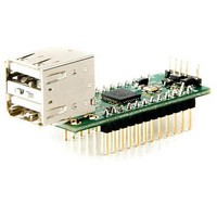
Manufacturer Part Number
V2DIP2-32
Description
Interface Modules & Development Tools USB Vinculum-II 32 Pin Mod 2 USB Ports
Manufacturer
FTDI
Datasheet
1.V2DIP2-32.pdf
(20 pages)
Specifications of V2DIP2-32
Interface Type
USB, Serial, UART, FIFO, SPI
Data Bus Width
Serial, 8 bit
Operating Supply Voltage
5 V
Product
Interface Modules
For Use With/related Products
VNC2-32
Lead Free Status / RoHS Status
Lead free / RoHS Compliant


When FIFO_WR# goes low FIFO_TXE# flag will always go high. FIFO_TXE# goes low again only when
there is still space for data to be written in to the module.
3.7 Debugger Interface
The purpose of the debugger interface is to provide access to the VNC2 silicon/firmware debugger. The
debug interface can be accessed via the J2-10 pin on the DIL connector or, more easily, it can be
accessed by connecting a VNC2_Debug_Module to the J3 connector. This debug module will give access
to the debugger through a USB connection to a PC via the Integrated Development Environment (IDE).
The IDE is a graphical interface to the VNC2 software development tool-chain and gives the following
debug capabilities through the debugger interface:
The Debugger Interface, and how to use it, is further described in the following applications Note
Vinculum-II Debug Interface Description
3.7.1 Signal Description - Debugger Interface
Table 3.8 shows the signals and pins description for the Debugger Interface pin header J3
J3-1
J3-2
J3-3
J3-4
J3-5
J3-6
Table 3.8 - Signal Name and Description – Debugger Interface
Pin No.
Flash Erase, Write and Program.
Application debug - application code can have breakpoints, be single stepped and can be halted.
Detailed internal debug - memory and register read/write access.
RESET#
PROG#
Name
GND
IO0
5V0
-
Copyright © 2010 Future Technology Devices International Limited
On PCB
Name
`
PRG#
[Key]
RST#
DBG
GND
VCC
PWR Input
V2DIP2-32 VNCL2-32Q Development Module Datasheet Version 1.0
Type
Input
Input
PWR
I/O
-
Can be used by an external device to reset the
VNCL2. This pin is also used in combination with
PROG# and the UART interface to program
firmware into the VNC2.
This pin is used in combination with the RESET#
pin and the UART interface to program firmware
into the VNC2.
5.0V module supply pin. This pin can be used to
provide the 5.0V input to the V2DIP2-32 from the
debugger interface when the V2DIP2-32 is not
powered from the USB connector (VBUs) or the
DIL connector pins J1-1 and J3-6.
Not connected. Used to make sure that the debug
module is connected correctly.
Module ground supply pin
Debugger Interface
Description
Document Reference No.: FT_000164
Clearance No.: FTDI# 151
12
Related parts for V2DIP2-32
Image
Part Number
Description
Manufacturer
Datasheet
Request
R

Part Number:
Description:
MOD MCU-USB HOST CTLR 40-DIP
Manufacturer:
FTDI, Future Technology Devices International Ltd
Datasheet:

Part Number:
Description:
MOD MCU-USB HOST CTLR 60-DIP
Manufacturer:
FTDI, Future Technology Devices International Ltd
Datasheet:

Part Number:
Description:
BOARD, EVALUATION, UK PSU
Manufacturer:
FTDI
Datasheet:
Part Number:
Description:
BOARD, EVALUATION, US PSU
Manufacturer:
FTDI
Datasheet:
Part Number:
Description:
Specifications: Manufacturer: FTDI ; Product Category: USB Interface IC ; RoHS: Details ; Operating Supply Voltage: 3 V to 5.25 V ; Supply Current: 25 mA ; Maximum Operating Temperature: + 70 C ; Mounting Style: SMD/SMT ; Package / Case: QFN-32
Manufacturer:
FTDI
Part Number:
Description:
integr. usb2.0/uart lqfp32 rohs ftdi reel c1k...
Manufacturer:
FTDI
Datasheet:
Part Number:
Description:
Interface Development Tools USB to UART Breakout Board
Manufacturer:
FTDI
Datasheet:

Part Number:
Description:
IC USB TO SERIAL UART 32-QFN
Manufacturer:
FTDI, Future Technology Devices International Ltd

Part Number:
Description:
USB Interface IC USB to Serial UART Enhanced IC SSOP-28
Manufacturer:
FTDI
Datasheet:

Part Number:
Description:
IC, USB UART INTERFACE, SSOP-28
Manufacturer:
FTDI
Datasheet:

Part Number:
Description:
IC, USB UART INTERFACE, QFN-32
Manufacturer:
FTDI
Datasheet:
Part Number:
Description:
IC, USB FIFO INTERFACE, SSOP-28
Manufacturer:
FTDI
Datasheet:
Part Number:
Description:
MODULE, USB, 4 PORT, FT4232H BASED
Manufacturer:
FTDI
Datasheet:
Part Number:
Description:
357-036-542-201 CARDEDGE 36POS DL .156 BLK LOPRO
Manufacturer:
FTDI
Datasheet:
Part Number:
Description:
357-036-542-201 CARDEDGE 36POS DL .156 BLK LOPRO
Manufacturer:
FTDI
Datasheet: