V2DIP1-32 FTDI, V2DIP1-32 Datasheet - Page 13
V2DIP1-32
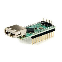
Manufacturer Part Number
V2DIP1-32
Description
Interface Modules & Development Tools USB Vinculum-II 32 Pin Mod 1 USB Port
Manufacturer
FTDI
Datasheet
1.V2DIP1-32.pdf
(21 pages)
Specifications of V2DIP1-32
Interface Type
USB, Serial, UART, FIFO, SPI
Data Bus Width
Serial, 8 bit
Operating Supply Voltage
5 V
Product
Interface Modules
For Use With/related Products
VNC2-32
Lead Free Status / RoHS Status
Lead free / RoHS Compliant


3.7 Debugger Interface
The purpose of the debugger interface is to provide access to the VNC2 silicon/firmware debugger. The
debug interface can be accessed via the J2-10 pin on the DIL connector or, more easily, it can be
accessed by connecting a VNC2_Debug_Module to the J3 connector. This debug module will give access
to the debugger through a USB connection to a PC via the Integrated Development Environment (IDE).
The IDE is a graphical interface to the VNC2 software development tool-chain and gives the following
debug capabilities through the debugger interface:
The Debugger Interface, and how to use it, is further described in the following applications Note
Vinculum-II Debug Interface Description
3.7.1 Signal Description - Debugger Interface
Table 3.8
Table 3.8 - Signal Name and Description – Debugger Interface
J3-1
J3-2
J3-3
J3-4
J3-5
J3-6
Pin No.
Flash Erase, Write and Program.
Application debug - application code can have breakpoints, be single stepped and can be halted.
Detailed internal debug - memory and register read/write access.
shows the signals and pins description for the Debugger Interface pin header J3
RESET#
PROG#
Name
GND
IO0
5V0
-
Copyright © 2010 Future Technology Devices International Limited
On PCB
Name
`
PRG#
[Key]
RST#
DBG
GND
VCC
PWR Input
Type
Input
Input
PWR
I/O
V2DIP1-32 VNC2-32Q Development Module Datasheet Version 1.0
-
Can be used by an external device to reset the
VNCL2. This pin is also used in combination with
PROG# and the UART interface to program
firmware into the VNC2.
This pin is used in combination with the RESET#
pin and the UART interface to program firmware
into the VNC2.
5.0V module supply pin. This pin can be used to
provide the 5.0V input to the V2DIP1-32 from the
debugger interface when the V2DIP1-32 is not
powered from the USB connector (VBUS) or the
DIL connector pins J1-1 and J3-6.
Not connected. Used to make sure that the debug
module is connected correctly.
Module ground supply pin
Debugger Interface
Description
Document Reference No.: FT_000163
Clearance No.: FTDI# 150
12
Related parts for V2DIP1-32
Image
Part Number
Description
Manufacturer
Datasheet
Request
R

Part Number:
Description:
MOD MCU-USB HOST CTLR 24-DIP
Manufacturer:
FTDI, Future Technology Devices International Ltd
Datasheet:

Part Number:
Description:
MOD MCU-USB HOST CTLR 60-DIP
Manufacturer:
FTDI, Future Technology Devices International Ltd
Datasheet:

Part Number:
Description:
BOARD, EVALUATION, UK PSU
Manufacturer:
FTDI
Datasheet:
Part Number:
Description:
BOARD, EVALUATION, US PSU
Manufacturer:
FTDI
Datasheet:
Part Number:
Description:
Specifications: Manufacturer: FTDI ; Product Category: USB Interface IC ; RoHS: Details ; Operating Supply Voltage: 3 V to 5.25 V ; Supply Current: 25 mA ; Maximum Operating Temperature: + 70 C ; Mounting Style: SMD/SMT ; Package / Case: QFN-32
Manufacturer:
FTDI
Part Number:
Description:
integr. usb2.0/uart lqfp32 rohs ftdi reel c1k...
Manufacturer:
FTDI
Datasheet:
Part Number:
Description:
Interface Development Tools USB to UART Breakout Board
Manufacturer:
FTDI
Datasheet:

Part Number:
Description:
IC USB TO SERIAL UART 32-QFN
Manufacturer:
FTDI, Future Technology Devices International Ltd

Part Number:
Description:
USB Interface IC USB to Serial UART Enhanced IC SSOP-28
Manufacturer:
FTDI
Datasheet:

Part Number:
Description:
IC, USB UART INTERFACE, SSOP-28
Manufacturer:
FTDI
Datasheet:

Part Number:
Description:
IC, USB UART INTERFACE, QFN-32
Manufacturer:
FTDI
Datasheet:
Part Number:
Description:
IC, USB FIFO INTERFACE, SSOP-28
Manufacturer:
FTDI
Datasheet:
Part Number:
Description:
MODULE, USB, 4 PORT, FT4232H BASED
Manufacturer:
FTDI
Datasheet:
Part Number:
Description:
357-036-542-201 CARDEDGE 36POS DL .156 BLK LOPRO
Manufacturer:
FTDI
Datasheet:
Part Number:
Description:
357-036-542-201 CARDEDGE 36POS DL .156 BLK LOPRO
Manufacturer:
FTDI
Datasheet: