TSL1412S TAOS, TSL1412S Datasheet - Page 2
TSL1412S
Manufacturer Part Number
TSL1412S
Description
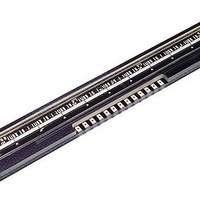
Photodiodes Linear Array 400 DPI
Manufacturer
TAOS
Type
Linear Sensor Arrayr
Datasheet
1.TSL1412S.pdf
(12 pages)
Specifications of TSL1412S
Peak Wavelength
640 nm
Maximum Rise Time
500 ns
Maximum Fall Time
500 ns
Maximum Operating Temperature
+ 70 C
Minimum Operating Temperature
0 C
Product
Photodiode
Lead Free Status / RoHS Status
Lead free / RoHS Compliant
Available stocks
Company
Part Number
Manufacturer
Quantity
Price
Company:

Part Number:
TSL1412S
Manufacturer:
MURATA
Quantity:
400 000


TSL1412S
1536 × 1 LINEAR SENSOR ARRAY WITH HOLD
TAOS045F − APRIL 2007
Terminal Functions
Detailed Description
2
Copyright E 2007, TAOS Inc.
AO1
AO2
CLK1
CLK2
GND
HOLD1
HOLD2
SI1
SI2
SO1
SO2
V
V
NAME
DD
PP
TERMINAL
The sensor consists of 1536 photodiodes, called pixels, arranged in a linear array. Light energy impinging on a pixel
generates photocurrent that is then integrated by the active integration circuitry associated with that pixel.
During the integration period, a sampling capacitor connects to the output of the integrator through an analog switch. The
amount of charge accumulated at each pixel is directly proportional to the light intensity on that pixel and the integration time.
The output and reset of the integrators are controlled by a 768-bit shift register and reset logic. An output cycle is initiated
by clocking in a logic 1 on SI. Another signal, called HOLD, is generated from the rising edge of SI1 when SI1 and HOLD1
are connected together. This causes all 768 sampling capacitors to be disconnected from their respective integrators and
starts an integrator reset period. As the SI pulse is clocked through the shift register, the charge stored on the sampling
capacitors is sequentially connected to a charge-coupled output amplifier that generates a voltage on analog output AO.
The integrator reset period ends 18 clock cycles after the SI pulse is clocked in. Then the next integration period begins.
On the 768
2 (when SO1 is connected to SI2). The rising edge of the 769
output AO of section 1 to high-impedance state. Similarly, SO2 is clocked out on the 1536
clock pulse is needed to terminate the SO2 pulse and return AO of Section 2 to the high-impedance state.
integration time is desired, the next SI pulse may be presented after a minimum delay of t
time) after the 1537
AO is an op amp-type output that does not require an external pull-down resistor. This design allows a rail-to-rail
output voltage swing.
for saturation light level.
The voltage developed at analog output (AO) is given by:
where:
A 0.1 μF bypass capacitor should be connected between V
V
V
R
E
t
NO.
int
12
10
11
13
out
drk
e
e
6
4
5
3
9
2
8
7
1
th
clock rising edge, the SI pulse is clocked out on the SO1 pin (section 1) and becomes the SI pulse for section
I/O
I/O
O
O
O
O
is the analog output voltage for white condition
is the analog output voltage for dark condition
is the device responsivity for a given wavelength of light given in V/(μJ/cm
is the incident irradiance in μW/cm
is integration time in seconds
I
I
I
I
I
I
Analog output, section 1.
Analog output, section 2.
Clock, section 1. CLK1 controls charge transfer, pixel output, and reset.
Clock, section 2. CLK2 controls charge transfer, pixel output, and reset.
Ground (substrate). All voltages are referenced to GND.
Hold signal. HOLD1 shifts pixel data to parallel buffer. HOLD1 is normally connected to SI1 and HOLD2 in
serial mode and to SI1 in parallel mode.
Hold signal. HOLD2 shifts pixel data to parallel buffer. HOLD2 is normally connected to SI2 in parallel mode.
Serial input (section 1). SI1 defines the start of the data-out sequence.
Serial input (section 2). SI2 defines the start of the data-out sequence.
Serial output (section 1). SO1 provides a signal to drive the SI2 input in serial mode.
Serial output (section 2). SO2 provides a signal to drive the SI input of another device for cascading or as an
end-of-data indication.
Supply voltage for both analog and digital circuitry.
Normally grounded.
th
With V
clock pulse.
When the device is not in the output phase, AO is in a high-impedance state.
DD
V
= 5 V, the output is nominally 0 V for no light input, 2 V for normal white level, and 4.8 V
out
Sections may be operated in parallel or in serial fashion.
= V
r
drk
+ (R
www.taosinc.com
e
2
) (E
e
)(t
int
th
)
clock cycle terminates the SO1 pulse, and returns the analog
DESCRIPTION
DESCRIPTION
DD
and ground as close as possible to the device.
r
th
2
clock pulse. Note that a 1537
The LUMENOLOGY r Company
)
qt
(pixel charge transfer
If a minimum
th
Related parts for TSL1412S
Image
Part Number
Description
Manufacturer
Datasheet
Request
R

Part Number:
Description:
Microcontroller Modules & Accessories TAOS Eval Module w/USB Interface
Manufacturer:
TAOS
Part Number:
Description:
Optical Sensor Development Tools TAOS Eval Module
Manufacturer:
TAOS

Part Number:
Description:
Industrial Optical Sensors Ambient Light Sensor SMBus
Manufacturer:
TAOS
Datasheet:

Part Number:
Description:
Photodiodes TriColor Sensor RGB, Clear Ch
Manufacturer:
TAOS
Datasheet:

Part Number:
Description:
LED Displays Hexadecimal Display 4-bit
Manufacturer:
TAOS
Datasheet:

Part Number:
Description:
Photodiodes Linear Sensor Array 200dpi 64pix
Manufacturer:
TAOS
Datasheet:

Part Number:
Description:
Industrial Optical Sensors Ambient Light Sensor SMBus
Manufacturer:
TAOS
Datasheet:

Part Number:
Description:
Photodiodes Linear Array 200 DPI
Manufacturer:
TAOS
Datasheet:

Part Number:
Description:
Photodiodes Light to Voltage Converter
Manufacturer:
TAOS
Datasheet:

Part Number:
Description:
Photodiodes Linear Array 200 DPI
Manufacturer:
TAOS
Datasheet:
Part Number:
Description:
Industrial Optical Sensors Ambient Light Sensor SMBus
Manufacturer:
TAOS
Datasheet:
Part Number:
Description:
Photodiodes TriColor Sensor RGB, Clear Ch
Manufacturer:
TAOS
Datasheet:
Part Number:
Description:
LED Displays Hexadecimal Display 4-bit
Manufacturer:
TAOS
Datasheet:
Part Number:
Description:
Photodiodes Linear Sensor Array 200dpi 64pix
Manufacturer:
TAOS
Datasheet:
