AD7298BCPZ Analog Devices Inc, AD7298BCPZ Datasheet - Page 4
AD7298BCPZ
Manufacturer Part Number
AD7298BCPZ
Description
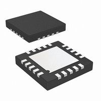
IC ADC 12BIT SPI/SRL 1M 20LFCSP
Manufacturer
Analog Devices Inc
Datasheet
1.AD7298BCPZ.pdf
(24 pages)
Specifications of AD7298BCPZ
Data Interface
Serial, SPI™
Featured Product
AD7298 ADC with Temperature Sensor
Number Of Bits
12
Sampling Rate (per Second)
1M
Number Of Converters
1
Power Dissipation (max)
22.7mW
Voltage Supply Source
Single Supply
Operating Temperature
-40°C ~ 125°C
Mounting Type
Surface Mount
Package / Case
20-WFQFN, CSP Exposed Pad
Resolution (bits)
12bit
Sampling Rate
1MSPS
Input Channel Type
Single Ended
Supply Voltage Range - Digital
1.65V To 3.6V
Supply Current
5.8mA
Digital Ic Case
RoHS Compliant
Supply Voltage Range - Analog
1.65V To 3.6V
Digital Ic Case Style
LFCSP
Rohs Compliant
Yes
Lead Free Status / RoHS Status
Lead free / RoHS Compliant
Available stocks
Company
Part Number
Manufacturer
Quantity
Price
Company:

Part Number:
AD7298BCPZ
Manufacturer:
Analog Devices Inc
Quantity:
135
Part Number:
AD7298BCPZ
Manufacturer:
ADI/亚德诺
Quantity:
20 000


AD7298
Parameter
LOGIC INPUTS
LOGIC OUTPUTS
TEMPERATURE SENSOR—INTERNAL
CONVERSION RATE
POWER REQUIREMENTS
1
2
3
4
5
6
7
See the Terminology Section.
All specifications expressed in decibels are referred to full-scale input, FSR, and tested with an input signal at 0.5 dB below full scale, unless otherwise specified.
Sample tested during initial release to ensure compliance.
Refers to Pin
A correction factor may be required on the temperature sensor results when using an external V
I
Power dissipation is specified with V
TOTAL
Floating State Leakage Current
Floating State Output Capacitance
I
Power Dissipation
Input High Voltage, V
Input Low Voltage, V
Input Current, I
Input Capacitance, C
Output High Voltage, V
Output Low Voltage, V
Operating Range
Accuracy
Resolution
Conversion Time
Track-and-Hold Acquisition Time
Throughput Rate
V
V
TOTAL
DD
DRIVE
Normal Mode (Operational)
Normal Mode (Static)
Partial Power-Down Mode
Full Power-Down Mode
Normal Mode (Operational)
Normal Mode (Static)
Partial Power-Down Mode
Full Power-Down Mode
is the total current flowing in V
6
V
REF
specified for 25
IN
7
INL
IN
INH
3
OL
OH
o
C.
DD
DD
and V
= V
3
DRIVE
3
DRIVE
= 3.6 V, unless otherwise noted.
.
Min
0.7 × V
V
V
−40
2.8
1.65
DRIVE
DRIVE
− 0.3
− 0.2
DRIVE
Rev. A | Page 4 of 24
Typ
±0.01
3
±0.01
8
±1
0.25
1
3
3
5.8
4.1
2.7
1
17.4
14.8
9.8
3.6
Max
+0.3 × V
±1
0.4
±1
+125
±3
t
100
100
1
10
3.6
3.6
6.3
4.6
3.3
1.6
10
18.9
22.7
16.6
11.9
5.8
36
2
+ 16 × t
DRIVE
REF
SCLK
(see the Temperature Sensor Averaging section).
Unit
V
V
μA
pF
V
V
V
μA
pF
°C
°C
μs
μs
ns
MSPS
KSPS
V
V
mA
mA
mA
μA
μA
mW
mW
mW
mW
μW
μW
Test Conditions/Comments
V
V
V
T
LSB size
For V
T
Full-scale step input
f
conversions, one cycle latency
For the T
Digital inputs = 0 V or V
V
T
T
T
T
V
SCLK
A
SENSE
A
A
A
A
IN
DRIVE
DRIVE
DD
DD
= −40°C to +125°C
= −40°C to +25°C
= −40°C to +125°C
= −40°C to +25°C
= −40°C to +125°C
= 0 V or V
= 3.6 V, V
= 3 V, V
= 20 MHz, for analog voltage
IN0
< 1.8
≥ 1.8
temperature sensor channel
to V
SENSE
DRIVE
IN7
DRIVE
DRIVE
channel, one cycle latency
, with one cycle latency
= 3 V
= 3.6 V
DRIVE
Related parts for AD7298BCPZ
Image
Part Number
Description
Manufacturer
Datasheet
Request
R

Part Number:
Description:
8Channel 10Bit SAR
Manufacturer:
Analog Devices Inc
Datasheet:

Part Number:
Description:
±1.7g Dual-Axis IMEMS Accelerometer Evaluation Board
Manufacturer:
Analog Devices Inc
Datasheet:

Part Number:
Description:
Inertial Sensor Evaluation System
Manufacturer:
Analog Devices Inc
Datasheet:
Part Number:
Description:
Manufacturer:
Analog Devices Inc
Datasheet:
Part Number:
Description:
Manufacturer:
Analog Devices Inc
Datasheet:
Part Number:
Description:
Manufacturer:
Analog Devices Inc
Datasheet:
Part Number:
Description:
Manufacturer:
Analog Devices Inc
Datasheet:
Part Number:
Description:
Manufacturer:
Analog Devices Inc
Datasheet:
Part Number:
Description:
Manufacturer:
Analog Devices Inc
Datasheet:
Part Number:
Description:
Manufacturer:
Analog Devices Inc
Datasheet:
Part Number:
Description:
Manufacturer:
Analog Devices Inc
Datasheet:
Part Number:
Description:
Manufacturer:
Analog Devices Inc
Datasheet: