TBU-PL060-200-WH Bourns Inc., TBU-PL060-200-WH Datasheet - Page 5
TBU-PL060-200-WH
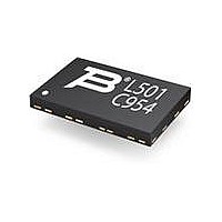
Manufacturer Part Number
TBU-PL060-200-WH
Description
SURGE SUPP TBU DL 50OHM 600VIMP
Manufacturer
Bourns Inc.
Series
TBU™r
Specifications of TBU-PL060-200-WH
Package / Case
SMD 6.50mm x 4.00mm
Voltage - Working
350V
Voltage - Clamping
600V
Technology
Mixed Technology
Number Of Circuits
2
Applications
SLIC
Voltage Rating
600 V
Current Rating
200 mA
Height
0.85 mm
Length
6.5 mm
Termination Style
SMD/SMT
Width
4 mm
Diode Type
Low Capacitance
Operating Voltage
-20V
Diode Case Style
DFN
No. Of Pins
8
Peak Surge Current
500A
Output Current
700µA
Suppressor Type
Transient Voltage
Rohs Compliant
Yes
Lead Free Status / RoHS Status
Lead free / RoHS Compliant
Power (watts)
-
Lead Free Status / Rohs Status
Lead free / RoHS Compliant
Other names
TBU-PL060-200-WHTR


TBU
tion fi nish. For improved thermal dissipation, the recommended
layout uses PCB copper areas which extend beyond the exposed
solder pad. The exposed solder pads should be defi ned by a
solder mask which matches the pad layout of the TBU
size and spacing. It is recommended that they should be the same
dimension as the TBU
they should be centered on the TBU
not more than 0.10-0.12 mm (0.004-0.005 in.) smaller in overall
width or length. Solder pad areas should not be larger than the
TBU
Dark grey areas show added PCB copper area for better
thermal resistance.
Specifi cations are subject to change without notice.
Customers should verify actual device performance in their specifi c applications.
Product Dimensions
Recommended Pad Layout
®
®
TBU-PL Series - TBU
High-Speed Protectors have a 100 % matte-tin termina-
pad sizes to ensure adequate clearance is maintained. The
(.157)
4.00
(.033)
0.85
®
4
5
pads but if smaller solder pads are used,
PIN 1 & BACKSIDE CHAMFER
6
3
(.256)
6.50
(.033)
0.85
7
2
®
package terminal pads and
®
(.035)
0.90
1
8
High-Speed Protectors
(.000 - .002)
0.00 - 0.05
(.031 - .037)
0.80 - 0.95
(.033 ± .002)
®
0.85 ± 0.05
device in
DIMENSIONS:
(.053)
1.335
(.053)
1.335
(.012)
0.30
recommended stencil thickness is 0.10-0.12 mm (0.004-0.005
in.) with a stencil opening size 0.025 mm (0.0010 in.) less than the
solder pad size. Extended copper areas beyond the solder pad
signifi cantly improve the junction to ambient thermal resistance,
resulting in operation at lower junction temperatures with a
corresponding benefi t of reliability. All pads should soldered to
the PCB, including pads marked as NC or NU but no electrical
connection should be made to these pads. For minimum parasitic
capacitance, it is recommended that signal, ground or power
signals are not routed beneath any pad.
Thermal Resistance vs Additional PCB Cu Area
(INCHES)
(.045)
(.049)
1.15
1.25
MM
(.030)
0.75
120
100
0.825
(.032)
80
60
40
20
(.029)
0
0.73
(.016)
0.40
(.028)
0.70
0
(.032)
0.825
(.053)
1.35
(.030)
(.028)
0.75
0.70
0.2
(.033)
(.016)
0.85
0.40
(.047)
1.20
(.047)
0.4
1.20
(.033)
0.85
(.053)
1.35
Power in One Side of TBU
Total Power in Both Sides of TBU
0.6
Added Cu Area (Sq. In.)
(.029)
(.033)
0.725
0.85
(.030)
0.75
0.8
(.050)
1.275
(.051)
1.0
1.30
(.012)
0.30
(.050)
(.050)
1.275
1.275
1.2
C
(.033)
(.010)
0.85
0.25
1.4
®
PIN 1
Device
1.6
®
Device
1.8
2.0
Related parts for TBU-PL060-200-WH
Image
Part Number
Description
Manufacturer
Datasheet
Request
R

Part Number:
Description:
SURGE SUPP TBU DL 50OHM 600VIMP
Manufacturer:
Bourns Inc.
Datasheet:

Part Number:
Description:
SLIC PROTECTION KIT
Manufacturer:
Bourns Inc.
Datasheet:

Part Number:
Description:
Manufacturer:
Bourns, Inc.
Datasheet:
Part Number:
Description:
11mm Potentiometer
Manufacturer:
Bourns, Inc.
Datasheet:
Part Number:
Description:
Manufacturer:
Bourns, Inc.
Datasheet:
Part Number:
Description:
Manufacturer:
Bourns, Inc.
Datasheet:
Part Number:
Description:
Manufacturer:
Bourns, Inc.
Datasheet:
Part Number:
Description:
5/16 Round Trimming Potentiometer
Manufacturer:
Bourns, Inc.
Datasheet:
Part Number:
Description:
4100R Series: Thick Film Moulded DIPs - Resistor Networks
Manufacturer:
Bourns, Inc.
Datasheet:
Part Number:
Description:
PROTECTOR - SINGLE BIDIRECTIONAL
Manufacturer:
Bourns, Inc.